This thread has been locked.

If you have a related question, please click the "Ask a related question" button in the top right corner. The newly created question will be automatically linked to this question.

CC2640R2F: Cannot program CC2640R2F: Unable to access the DAP

Part Number: CC2640R2F
Other Parts Discussed in Thread: LAUNCHXL-CC2640R2, , UNIFLASH, SYSCONFIG

Hello,

we have developed a custom board featuring the CC2640R2F SoC that can be programmed via a XDS110 on the LAUNCHXL-CC2640R2 board.  A while ago, I could program and debug the chip without any problems. This was valid for the newest revision of the board as well as the previous one. Now, suddenly, I'm not able to program any of the custom boards anymore. When I write the program into the on-board CC2640R2F on the launchpad by using jumpers to connect the same signals used on our board (+3.3V, GND, TCK, TMS, RESET) involving the same target configuration (CC2640R2F.ccxml), it works without problems. But when I attach our board, it won't work and displays a repeating error that it cannot access the DAP:

Flashloader: Verbose output enabled.
Writing Flash @ Address 0x00000000 of Length 0x00007ff0
Loading flashloader to target: FlashLoaderCC26x0.out 
  Chunk 1: addr=0x00000000, length=4096, crc=0x1938B2EE (using block 0)
Error: (Error -1170 @ 0x0) Unable to access the DAP. Reset the device, and retry the operation. If error persists, confirm configuration, power-cycle the board, and/or try more reliable JTAG settings (e.g. lower TCLK). (Emulation package 20.3.0.3656) 
Trouble Halting Target CPU: (Error -2064 @ 0x0) Unable to read device status. Reset the device, and retry the operation. If error persists, confirm configuration, power-cycle the board, and/or try more reliable JTAG settings (e.g. lower TCLK). (Emulation package 20.3.0.3656) 
Error: (Error -1170 @ 0x0) Unable to access the DAP. Reset the device, and retry the operation. If error persists, confirm configuration, power-cycle the board, and/or try more reliable JTAG settings (e.g. lower TCLK). (Emulation package 20.3.0.3656) 
Trouble Halting Target CPU: (Error -2064 @ 0x0) Unable to read device status. Reset the device, and retry the operation. If error persists, confirm configuration, power-cycle the board, and/or try more reliable JTAG settings (e.g. lower TCLK). (Emulation package 20.3.0.3656) 


Flashloader: Verbose output enabled.
Writing Flash @ Address 0x00000000 of Length 0x00007ff0
Loading flashloader to target: FlashLoaderCC26x0.out
   Chunk 1: addr=0x00000000, length=4096, crc=0x1938B2EE (using block 0)
   Chunk 2: addr=0x00001000, length=4096, crc=0x1FAA55EF (using block 1)
   Chunk 3: addr=0x00002000, length=4096, crc=0x508BA633 (using block 0)
   Chunk 4: addr=0x00003000, length=4096, crc=0xB74B9D9B (using block 1)
   Chunk 5: addr=0x00004000, length=4096, crc=0x747317C8 (using block 0)
   Chunk 6: addr=0x00005000, length=4096, crc=0x1BECAEA5 (using block 1)
   Chunk 7: addr=0x00006000, length=4096, crc=0x410894F7 (using block 0)
   Chunk 8: addr=0x00007000, length=4080, crc=0xEACB68DE (using block 1)
Writing Flash @ Address 0x00007ff0 of Length 0x00007ff0
   Chunk 1: addr=0x00007FF0, length=4096, crc=0xA10FBAB4 (using block 0)
   Chunk 2: addr=0x00008FF0, length=4096, crc=0x1FECFA8B (using block 1)
   Command=20 -- addr=0x00008FF0 -- length=0x00001000
Trouble Halting Target CPU: (Error -2064 @ 0x0) Unable to read device
status. Reset the device, and retry the operation. If error persists,
confirm configuration, power-cycle the board, and/or try more reliable
JTAG settings (e.g. lower TCLK). (Emulation package 20.3.0.3656)
Error: (Error -1170 @ 0x0) Unable to access the DAP. Reset the device,
and retry the operation. If error persists, confirm configuration,
power-cycle the board, and/or try more reliable JTAG settings (e.g.
lower TCLK). (Emulation package 20.3.0.3656)
Trouble Halting Target CPU: (Error -2064 @ 0x0) Unable to read device
status. Reset the device, and retry the operation. If error persists,
confirm configuration, power-cycle the board, and/or try more reliable
JTAG settings (e.g. lower TCLK). (Emulation package 20.3.0.3656)

Sometimes, the error number is different (as seen above), and a part of the code gets loaded. But even then, it stopped at the same point on every single try.

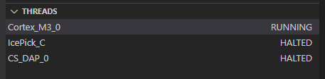
The weird thing is - when I connect to the interface manually, I don't experience any problems. I can connect to the board, show all cores, and connect to the Cortex M3, the DAP as well as the IcePick. 

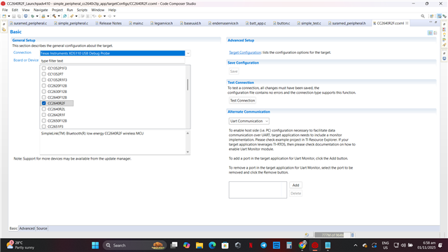
I also tried unplugging and re-plugging all cables, lowering the TCLK to 1.5 MHz, and did various JTAG connectivity tests. Those work without a problem:

Test Connections
-----[Print the board config pathname(s)]------------------------------------ C:\Users\Arbeit\AppData\Local\TEXASI~1\CCS\ ccs2031\0\0\BrdDat\testBoard.dat -----[Print the reset-command software log-file]----------------------------- This utility has selected a 100/110/510 class product. This utility will load the adapter 'jioxds110.dll'. The library build date was 'Aug 12 2025'. The library build time was '02:44:21'. The library package version is '20.3.0.3656'. The library component version is '35.35.0.0'. The controller does not use a programmable FPGA. The controller has a version number of '5' (0x00000005). The controller has an insertion length of '0' (0x00000000). This utility will attempt to reset the controller. This utility has successfully reset the controller. -----[Print the reset-command hardware log-file]----------------------------- The scan-path will be reset by toggling the JTAG TRST signal. The controller is the XDS110 with USB interface. The link from controller to target is direct (without cable). The software is configured for XDS110 features. The controller cannot monitor the value on the EMU[0] pin. The controller cannot monitor the value on the EMU[1] pin. The controller cannot control the timing on output pins. The controller cannot control the timing on input pins. The scan-path link-delay has been set to exactly '0' (0x0000). -----[Perform the Integrity scan-test on the JTAG IR]------------------------ This test will use blocks of 64 32-bit words. This test will be applied just once. Do a test using 0xFFFFFFFF. Scan tests: 1, skipped: 0, failed: 0 Do a test using 0x00000000. Scan tests: 2, skipped: 0, failed: 0 Do a test using 0xFE03E0E2. Scan tests: 3, skipped: 0, failed: 0 Do a test using 0x01FC1F1D. Scan tests: 4, skipped: 0, failed: 0 Do a test using 0x5533CCAA. Scan tests: 5, skipped: 0, failed: 0 Do a test using 0xAACC3355. Scan tests: 6, skipped: 0, failed: 0 All of the values were scanned correctly. The JTAG IR Integrity scan-test has succeeded. -----[Perform the Integrity scan-test on the JTAG DR]------------------------ This test will use blocks of 64 32-bit words. This test will be applied just once. Do a test using 0xFFFFFFFF. Scan tests: 1, skipped: 0, failed: 0 Do a test using 0x00000000. Scan tests: 2, skipped: 0, failed: 0 Do a test using 0xFE03E0E2. Scan tests: 3, skipped: 0, failed: 0 Do a test using 0x01FC1F1D. Scan tests: 4, skipped: 0, failed: 0 Do a test using 0x5533CCAA. Scan tests: 5, skipped: 0, failed: 0 Do a test using 0xAACC3355. Scan tests: 6, skipped: 0, failed: 0 All of the values were scanned correctly. The JTAG DR Integrity scan-test has succeeded.
Compiler is TI v18.12.5 LTS
XDCTools 5.51.3.28_core
SimpleLink CC2640R2F SDK 5.30.0.03
 
I can't think of anything that could be wrong. I would be very happy for any help and hints - Please let me know if you need any more information. Thank you very much in advance! :)
 
best wishes,
Nico
  • Hello Nico,

    Sometimes, the error number is different (as seen above), and a part of the code gets loaded. But even then, it stopped at the same point on every single try.

    The weird thing is - when I connect to the interface manually, I don't experience any problems. I can connect to the board, show all cores, and connect to the Cortex M3, the DAP as well as the IcePick. 

    Can you expand on "when I connect the interface manually, I don't experience any problems"?

    What is the difference to the above statement vs the below? In both cases we are attaching them manually, no?

    using jumpers to connect the same signals used on our board (+3.3V, GND, TCK, TMS, RESET) involving the same target configuration (CC2640R2F.ccxml), it works without problems. But when I attach our board, it won't work and displays a repeating error that it cannot access the DAP:

    Flashloader: Verbose output enabled.

    Have you already had your custom PCB reviewed by TIs design review forum? 

    Thanks,
    Alex F

  • A while ago, I could program and debug the chip without any problems. This was valid for the newest revision of the board as well as the previous one. Now, suddenly, I'm not able to program any of the custom boards anymore.

    If you are programming using the P4 of the CC2640R2F Launchpad pins +3.3V, GND, TCK, TMS, RESET, you might need to scrape the pins using cutter to make sure there are no dirt or corrosion on the pins. You also need to check the wires if there is connectivity. Also make sure the wires are not too long.

    If this does not work then it is possible that your custom boards have developed a problem which would need to be investigated.

    -kel 

  • Hey Alex,

    thanks for reaching out!
    In the first statement, I was talking about manually connecting to the custom board. When I enter the debug workspace and just start the target configuration for our board, I can connect to all mentioned parts of the SoC:

    Still, when I want to load the program into the board, the error above occurs, saying it is not possible to talk to the DAP; still, this view shows that I am somehow able to connect to the DAP. Also, both of my two working prototypes of different design iterations "broke" at the same time, so I suspected that it is a fault that somehow might have to do with the launchpad used for programming or the CCS IDE.
    And yes, we had our design reviewed a while ago by your team, but via Mail :)

    best wishes,
    Nico

  • Hey Markel, 

    thak you very much for the hint! I will try that. Still, I doubt that it might help too much, because the on-board SoC gets connected to the programmer via the same jumpers. Shouldn't the same effect happen here, too? Will come back here and say if it worked :) 

    best wishes,
    Nico

  • Hello Nico,

    this view shows that I am somehow able to connect to the DAP.

    Correct, this seems like you can at least enter a debug session, as a double check can you open UniFlash and attempt to read the memory or see if you can manually completely erase the device? 

    both of my two working prototypes of different design iterations "broke" at the same time, so I suspected that it is a fault that somehow might have to do with the launchpad used for programming or the CCS IDE.

    The XDS is what programs the board, not the LaunchPad itself; what did you set your device permission settings in Sysconfig to? 

    Seeing as both of the board "broke at the same time" did you program the same image to both, or were these two completely separate images? 

    Again lets try to see if the UniFlash tool can first connect to the device, then do a full mass erase of the device and try to re-flash it to see it starts working again.

    Thanks,
    Alexander F

  • Hi,

    See, Cannot access the DAP Error -1170 from the link below. This is usually caused by either a hardware failure on the board or invalid code on the subcore that causes it to reset itself continuously..

    https://software-dl.ti.com/ccs/esd/documents/ccs_debugging_jtag_connectivity_issues.html#cannot-access-the-dap

    This should be not a problem if you use one of the example programs in the SDK as base for your program. 

    Also make sure the target board is set to CC2640R2F.

    -kel

  • Thank you very much! This indeed worked. I was able to re-program the chip after the mass erase, only to find out the same error occurred again (and was able to be mitigated by the same procedure again).
    Sadly, I now get this error:

    IcePick_C: Error connecting to the target: (Error -241 @ 0x0) A router subpath could not be accessed. A security error has probably occurred. Make sure your device is unlocked. (Emulation package 20.3.0.3656) 


    As I read from the forums, it might have something to do with the clock. From what I saw until now, the clock should be fine; still, I will check on that more thoroughly.

    best wishes,
    Nico

  • Hello Nico,

    I did want to mention that there is a case where if we mass erase the device (both application and CCFG) and attempt to flash the device with a project that has the debug authorization set to anything but always allowed that the programming will fail due to "security/debug". 

    The reason here is that the new project wants to check the CCFG (which is blank) for if debug is set to password/hash protected but can't find any information so it defaults to assuming it can't flash the device. 

    The solution when the device is mass erased is the flash any project that has the debug set to always allowed, then flash your project that has the debug authorization required.  

    However if your current project is set to always authorized and you are getting the error above that is likely a separate issue we should look into. 

    Thanks,
    Alex F

  • Hello Alex,

    this sounds indeed like something that could be the case! Thank you ver ymuch for the tip.
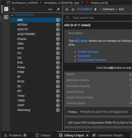
    I tried to find the options for that; sadly, when I create a new SysCfg, I only get a few options and no debug configuration preferences at all:

    According to the article here, there should be plenty more. What's wrong in my case?
    And do you need any more information to be able to help me find the cause? Like, other config files?

    best wishes,
    Nico

  • Follow-up - Maybe it's still something different. If I could program the board with the correct debug configuration, then I should also be able to mass-erase or blank check the chip via Uniflash, which is sadls not the case. I also get the following error here:


    Error connecting to the target: (Error -241 @ 0x0) A router subpath could not be accessed. A security error has probably occurred. Make sure your device is unlocked. (Emulation package 20.3.0.3656)

  • Hello Nico,

    The debug authorization (password) seems to not be settable on the CC2640R2 it seems, instead it has debug allowed or not allowed.

    On the topic of device settings we would have to look into the .ccfg file (or your device configuration file). 

    //#####################################
    // Debug access settings
    //#####################################
    
    #ifndef SET_CCFG_CCFG_TI_OPTIONS_TI_FA_ENABLE
    #define SET_CCFG_CCFG_TI_OPTIONS_TI_FA_ENABLE           0x00       // Disable unlocking of TI FA option.
    // #define SET_CCFG_CCFG_TI_OPTIONS_TI_FA_ENABLE        0xC5       // Enable unlocking of TI FA option with the unlock code
    #endif
    
    #ifndef SET_CCFG_CCFG_TAP_DAP_0_CPU_DAP_ENABLE
    // #define SET_CCFG_CCFG_TAP_DAP_0_CPU_DAP_ENABLE       0x00       // Access disabled
    #define SET_CCFG_CCFG_TAP_DAP_0_CPU_DAP_ENABLE          0xC5       // Access enabled if also enabled in FCFG
    #endif
    
    #ifndef SET_CCFG_CCFG_TAP_DAP_0_PRCM_TAP_ENABLE
    #define SET_CCFG_CCFG_TAP_DAP_0_PRCM_TAP_ENABLE         0x00       // Access disabled
    // #define SET_CCFG_CCFG_TAP_DAP_0_PRCM_TAP_ENABLE      0xC5       // Access enabled if also enabled in FCFG
    #endif
    
    #ifndef SET_CCFG_CCFG_TAP_DAP_0_TEST_TAP_ENABLE
    // #define SET_CCFG_CCFG_TAP_DAP_0_TEST_TAP_ENABLE      0x00       // Access disabled
    #define SET_CCFG_CCFG_TAP_DAP_0_TEST_TAP_ENABLE         0xC5       // Access enabled if also enabled in FCFG
    #endif
    
    #ifndef SET_CCFG_CCFG_TAP_DAP_1_PBIST2_TAP_ENABLE
    #define SET_CCFG_CCFG_TAP_DAP_1_PBIST2_TAP_ENABLE       0x00       // Access disabled
    // #define SET_CCFG_CCFG_TAP_DAP_1_PBIST2_TAP_ENABLE    0xC5       // Access enabled if also enabled in FCFG
    #endif
    
    #ifndef SET_CCFG_CCFG_TAP_DAP_1_PBIST1_TAP_ENABLE
    #define SET_CCFG_CCFG_TAP_DAP_1_PBIST1_TAP_ENABLE       0x00       // Access disabled
    // #define SET_CCFG_CCFG_TAP_DAP_1_PBIST1_TAP_ENABLE    0xC5       // Access enabled if also enabled in FCFG
    #endif
    
    #ifndef SET_CCFG_CCFG_TAP_DAP_1_WUC_TAP_ENABLE
    #define SET_CCFG_CCFG_TAP_DAP_1_WUC_TAP_ENABLE          0x00       // Access disabled
    // #define SET_CCFG_CCFG_TAP_DAP_1_WUC_TAP_ENABLE       0xC5       // Access enabled if also enabled in FCFG
    #endif

    I also get the following error here:

    -If the device debug, and device flash is both set to disabled we may not be able to erase the device, we could try to see if we can enter the ROM serial bootloader and command it to do a chip erase request. 

    Thanks,
    Alex F

  • Hello Alex,

    my CCFG indeed looks the same in the debug section. I'll try to change everything to "enabled if also enabled in FCFG" later when I have access to the hardware again. Thanks for the hint!

    /******************************************************************************
    
     @file  ccfg_app_ble_rcosc.c
    
     @brief Customer Configuration for CC26xx device family (HW rev 2) using RCOSC
    
     Group: WCS, BTS
     Target Device: cc2640r2
    
     ******************************************************************************
     
     Copyright (c) 2016-2021, Texas Instruments Incorporated
     All rights reserved.
    
     Redistribution and use in source and binary forms, with or without
     modification, are permitted provided that the following conditions
     are met:
    
     *  Redistributions of source code must retain the above copyright
        notice, this list of conditions and the following disclaimer.
    
     *  Redistributions in binary form must reproduce the above copyright
        notice, this list of conditions and the following disclaimer in the
        documentation and/or other materials provided with the distribution.
    
     *  Neither the name of Texas Instruments Incorporated nor the names of
        its contributors may be used to endorse or promote products derived
        from this software without specific prior written permission.
    
     THIS SOFTWARE IS PROVIDED BY THE COPYRIGHT HOLDERS AND CONTRIBUTORS "AS IS"
     AND ANY EXPRESS OR IMPLIED WARRANTIES, INCLUDING, BUT NOT LIMITED TO,
     THE IMPLIED WARRANTIES OF MERCHANTABILITY AND FITNESS FOR A PARTICULAR
     PURPOSE ARE DISCLAIMED. IN NO EVENT SHALL THE COPYRIGHT OWNER OR
     CONTRIBUTORS BE LIABLE FOR ANY DIRECT, INDIRECT, INCIDENTAL, SPECIAL,
     EXEMPLARY, OR CONSEQUENTIAL DAMAGES (INCLUDING, BUT NOT LIMITED TO,
     PROCUREMENT OF SUBSTITUTE GOODS OR SERVICES; LOSS OF USE, DATA, OR PROFITS;
     OR BUSINESS INTERRUPTION) HOWEVER CAUSED AND ON ANY THEORY OF LIABILITY,
     WHETHER IN CONTRACT, STRICT LIABILITY, OR TORT (INCLUDING NEGLIGENCE OR
     OTHERWISE) ARISING IN ANY WAY OUT OF THE USE OF THIS SOFTWARE,
     EVEN IF ADVISED OF THE POSSIBILITY OF SUCH DAMAGE.
    
     ******************************************************************************
     
     
     *****************************************************************************/
    
    #include <stdint.h>
    #include <inc/hw_types.h>
    #include <inc/hw_ccfg.h>
    #include <inc/hw_ccfg_simple_struct.h>
    
    //*****************************************************************************
    //
    // Introduction
    //
    // This file contains fields used by Boot ROM, startup code, and SW radio
    // stacks to configure chip behavior.
    //
    // Fields are documented in more details in hw_ccfg.h and CCFG.html in
    // DriverLib documentation (doc_overview.html -> CPU Domain Memory Map -> CCFG).
    //
    //*****************************************************************************
    
    //*****************************************************************************
    //
    // Set the values of the individual bit fields.
    //
    //*****************************************************************************
    
    //#####################################
    // Alternative DC/DC settings
    //#####################################
    
    #ifndef SET_CCFG_SIZE_AND_DIS_FLAGS_DIS_ALT_DCDC_SETTING
    #define SET_CCFG_SIZE_AND_DIS_FLAGS_DIS_ALT_DCDC_SETTING    0x0    // Alternative DC/DC setting enabled
    // #define SET_CCFG_SIZE_AND_DIS_FLAGS_DIS_ALT_DCDC_SETTING 0x1    // Alternative DC/DC setting disabled
    #endif
    
    #ifndef SET_CCFG_MODE_CONF_1_ALT_DCDC_VMIN
    #define SET_CCFG_MODE_CONF_1_ALT_DCDC_VMIN              0x8        // 2.25V
    #endif
    
    #ifndef SET_CCFG_MODE_CONF_1_ALT_DCDC_DITHER_EN
    #define SET_CCFG_MODE_CONF_1_ALT_DCDC_DITHER_EN         0x0        // Disable
    // #define SET_CCFG_MODE_CONF_1_ALT_DCDC_DITHER_EN      0x1        // Enable
    #endif
    
    #ifndef SET_CCFG_MODE_CONF_1_ALT_DCDC_IPEAK
    #define SET_CCFG_MODE_CONF_1_ALT_DCDC_IPEAK             0x2        // 39mA
    #endif
    
    //#####################################
    // XOSC override settings
    //#####################################
    
    #ifndef SET_CCFG_SIZE_AND_DIS_FLAGS_DIS_XOSC_OVR
    // #define SET_CCFG_SIZE_AND_DIS_FLAGS_DIS_XOSC_OVR     0x0        // Enable override
    #define SET_CCFG_SIZE_AND_DIS_FLAGS_DIS_XOSC_OVR        0x1        // Disable override
    #endif
    
    #ifndef SET_CCFG_MODE_CONF_1_DELTA_IBIAS_INIT
    #define SET_CCFG_MODE_CONF_1_DELTA_IBIAS_INIT           0x0        // Delta = 0
    #endif
    
    #ifndef SET_CCFG_MODE_CONF_1_DELTA_IBIAS_OFFSET
    #define SET_CCFG_MODE_CONF_1_DELTA_IBIAS_OFFSET         0x0        // Delta = 0
    #endif
    
    #ifndef SET_CCFG_MODE_CONF_1_XOSC_MAX_START
    #define SET_CCFG_MODE_CONF_1_XOSC_MAX_START             0x10       // 1600us
    #endif
    
    //#####################################
    // Power settings
    //#####################################
    
    #ifndef SET_CCFG_MODE_CONF_VDDR_TRIM_SLEEP_DELTA
    #define SET_CCFG_MODE_CONF_VDDR_TRIM_SLEEP_DELTA        0xF        // Signed delta value +1 to apply to the VDDR_TRIM_SLEEP target (0xF=-1=default=no compensation)
    #endif
    
    #ifndef SET_CCFG_MODE_CONF_DCDC_RECHARGE
    #define SET_CCFG_MODE_CONF_DCDC_RECHARGE                0x0        // Use the DC/DC during recharge in powerdown
    // #define SET_CCFG_MODE_CONF_DCDC_RECHARGE             0x1        // Do not use the DC/DC during recharge in powerdown
    #endif
    
    #ifndef SET_CCFG_MODE_CONF_DCDC_ACTIVE
    #define SET_CCFG_MODE_CONF_DCDC_ACTIVE                  0x0        // Use the DC/DC during active mode
    // #define SET_CCFG_MODE_CONF_DCDC_ACTIVE               0x1        // Do not use the DC/DC during active mode
    #endif
    
    #ifndef SET_CCFG_MODE_CONF_VDDS_BOD_LEVEL
    // #define SET_CCFG_MODE_CONF_VDDS_BOD_LEVEL            0x0        // VDDS BOD level is 2.0V
    #define SET_CCFG_MODE_CONF_VDDS_BOD_LEVEL               0x1        // VDDS BOD level is 1.8V (or 1.65V for external regulator mode)
    #endif
    
    #ifndef SET_CCFG_MODE_CONF_VDDR_CAP
    #define SET_CCFG_MODE_CONF_VDDR_CAP                     0x3A       // Unsigned 8-bit integer representing the min. decoupling capacitance on VDDR in units of 100nF
    #endif
    
    #ifndef SET_CCFG_MODE_CONF_VDDR_TRIM_SLEEP_TC
    //#define SET_CCFG_MODE_CONF_VDDR_TRIM_SLEEP_TC           0x1        // Temperature compensation on VDDR sleep trim disabled (default)
     #define SET_CCFG_MODE_CONF_VDDR_TRIM_SLEEP_TC        0x0        // Temperature compensation on VDDR sleep trim enabled
    #endif
    
    //#####################################
    // Clock settings
    //#####################################
    
    #ifndef SET_CCFG_MODE_CONF_SCLK_LF_OPTION
    // #define SET_CCFG_MODE_CONF_SCLK_LF_OPTION          0x0        // LF clock derived from High Frequency XOSC
    // #define SET_CCFG_MODE_CONF_SCLK_LF_OPTION          0x1        // External LF clock
    //#define SET_CCFG_MODE_CONF_SCLK_LF_OPTION           0x2        // LF XOSC
     #define SET_CCFG_MODE_CONF_SCLK_LF_OPTION            0x3        // LF RCOSC
    #endif
    
    #ifndef SET_CCFG_MODE_CONF_XOSC_CAP_MOD
    // #define SET_CCFG_MODE_CONF_XOSC_CAP_MOD              0x0        // Apply cap-array delta
    #define SET_CCFG_MODE_CONF_XOSC_CAP_MOD                 0x1        // Don't apply cap-array delta
    #endif
    
    #ifndef SET_CCFG_MODE_CONF_XOSC_CAPARRAY_DELTA
    #define SET_CCFG_MODE_CONF_XOSC_CAPARRAY_DELTA          0xFF       // Signed 8-bit value, directly modifying trimmed XOSC cap-array value
    #endif
    
    #ifndef SET_CCFG_EXT_LF_CLK_DIO
    #define SET_CCFG_EXT_LF_CLK_DIO                         0x01       // DIO number if using external LF clock
    #endif
    
    #ifndef SET_CCFG_EXT_LF_CLK_RTC_INCREMENT
    #define SET_CCFG_EXT_LF_CLK_RTC_INCREMENT               0x800000   // RTC increment representing the external LF clock frequency
    #endif
    
    //#####################################
    // Special HF clock source setting
    //#####################################
    #ifndef SET_CCFG_MODE_CONF_XOSC_FREQ
    // #define SET_CCFG_MODE_CONF_XOSC_FREQ                 0x1        // Use HPOSC as HF source (if executing on a HPOSC chip, otherwise using default (=0x3))
    // #define SET_CCFG_MODE_CONF_XOSC_FREQ                 0x2        // HF source is a 48 MHz xtal
    #define SET_CCFG_MODE_CONF_XOSC_FREQ                    0x3        // HF source is a 24 MHz xtal (default)
    #endif
    
    //#####################################
    // Bootloader settings
    //#####################################
    
    #ifndef SET_CCFG_BL_CONFIG_BOOTLOADER_ENABLE
    #define SET_CCFG_BL_CONFIG_BOOTLOADER_ENABLE            0x00       // Disable ROM boot loader
    // #define SET_CCFG_BL_CONFIG_BOOTLOADER_ENABLE         0xC5       // Enable ROM boot loader
    #endif
    
    #ifndef SET_CCFG_BL_CONFIG_BL_LEVEL
    // #define SET_CCFG_BL_CONFIG_BL_LEVEL                  0x0        // Active low to open boot loader backdoor
    #define SET_CCFG_BL_CONFIG_BL_LEVEL                     0x1        // Active high to open boot loader backdoor
    #endif
    
    #ifndef SET_CCFG_BL_CONFIG_BL_PIN_NUMBER
    #define SET_CCFG_BL_CONFIG_BL_PIN_NUMBER                0xFF       // DIO number for boot loader backdoor
    #endif
    
    #ifndef SET_CCFG_BL_CONFIG_BL_ENABLE
    // #define SET_CCFG_BL_CONFIG_BL_ENABLE                 0xC5       // Enabled boot loader backdoor
    #define SET_CCFG_BL_CONFIG_BL_ENABLE                    0xFF       // Disabled boot loader backdoor
    #endif
    
    //#####################################
    // Debug access settings
    //#####################################
    
    #ifndef SET_CCFG_CCFG_TI_OPTIONS_TI_FA_ENABLE
    #define SET_CCFG_CCFG_TI_OPTIONS_TI_FA_ENABLE           0x00       // Disable unlocking of TI FA option.
    // #define SET_CCFG_CCFG_TI_OPTIONS_TI_FA_ENABLE        0xC5       // Enable unlocking of TI FA option with the unlock code
    #endif
    
    #ifndef SET_CCFG_CCFG_TAP_DAP_0_CPU_DAP_ENABLE
    // #define SET_CCFG_CCFG_TAP_DAP_0_CPU_DAP_ENABLE       0x00       // Access disabled
    #define SET_CCFG_CCFG_TAP_DAP_0_CPU_DAP_ENABLE          0xC5       // Access enabled if also enabled in FCFG
    #endif
    
    #ifndef SET_CCFG_CCFG_TAP_DAP_0_PRCM_TAP_ENABLE
    #define SET_CCFG_CCFG_TAP_DAP_0_PRCM_TAP_ENABLE         0x00       // Access disabled
    // #define SET_CCFG_CCFG_TAP_DAP_0_PRCM_TAP_ENABLE      0xC5       // Access enabled if also enabled in FCFG
    #endif
    
    #ifndef SET_CCFG_CCFG_TAP_DAP_0_TEST_TAP_ENABLE
    // #define SET_CCFG_CCFG_TAP_DAP_0_TEST_TAP_ENABLE      0x00       // Access disabled
    #define SET_CCFG_CCFG_TAP_DAP_0_TEST_TAP_ENABLE         0xC5       // Access enabled if also enabled in FCFG
    #endif
    
    #ifndef SET_CCFG_CCFG_TAP_DAP_1_PBIST2_TAP_ENABLE
    #define SET_CCFG_CCFG_TAP_DAP_1_PBIST2_TAP_ENABLE       0x00       // Access disabled
    // #define SET_CCFG_CCFG_TAP_DAP_1_PBIST2_TAP_ENABLE    0xC5       // Access enabled if also enabled in FCFG
    #endif
    
    #ifndef SET_CCFG_CCFG_TAP_DAP_1_PBIST1_TAP_ENABLE
    #define SET_CCFG_CCFG_TAP_DAP_1_PBIST1_TAP_ENABLE       0x00       // Access disabled
    // #define SET_CCFG_CCFG_TAP_DAP_1_PBIST1_TAP_ENABLE    0xC5       // Access enabled if also enabled in FCFG
    #endif
    
    #ifndef SET_CCFG_CCFG_TAP_DAP_1_WUC_TAP_ENABLE
    #define SET_CCFG_CCFG_TAP_DAP_1_WUC_TAP_ENABLE          0x00       // Access disabled
    // #define SET_CCFG_CCFG_TAP_DAP_1_WUC_TAP_ENABLE       0xC5       // Access enabled if also enabled in FCFG
    #endif
    
    //#####################################
    // Alternative IEEE 802.15.4 MAC address
    //#####################################
    #ifndef SET_CCFG_IEEE_MAC_0
    #define SET_CCFG_IEEE_MAC_0                             0xFFFFFFFF // Bits [31:0]
    #endif
    
    #ifndef SET_CCFG_IEEE_MAC_1
    #define SET_CCFG_IEEE_MAC_1                             0xFFFFFFFF // Bits [63:32]
    #endif
    
    //#####################################
    // Alternative BLE address
    //#####################################
    #ifndef SET_CCFG_IEEE_BLE_0
    #define SET_CCFG_IEEE_BLE_0                             0xFFFFFFFF // Bits [31:0]
    #endif
    
    #ifndef SET_CCFG_IEEE_BLE_1
    #define SET_CCFG_IEEE_BLE_1                             0xFFFFFFFF // Bits [63:32]
    #endif
    
    //#####################################
    // Flash erase settings
    //#####################################
    
    #ifndef SET_CCFG_ERASE_CONF_CHIP_ERASE_DIS_N
    // #define SET_CCFG_ERASE_CONF_CHIP_ERASE_DIS_N         0x0        // Any chip erase request detected during boot will be ignored
    #define SET_CCFG_ERASE_CONF_CHIP_ERASE_DIS_N            0x1        // Any chip erase request detected during boot will be performed by the boot FW
    #endif
    
    #ifndef SET_CCFG_ERASE_CONF_BANK_ERASE_DIS_N
    // #define SET_CCFG_ERASE_CONF_BANK_ERASE_DIS_N         0x0        // Disable the boot loader bank erase function
    #define SET_CCFG_ERASE_CONF_BANK_ERASE_DIS_N            0x1        // Enable the boot loader bank erase function
    #endif
    
    //#####################################
    // Flash image valid
    //#####################################
    #ifndef SET_CCFG_IMAGE_VALID_CONF_IMAGE_VALID
    #define SET_CCFG_IMAGE_VALID_CONF_IMAGE_VALID           0x00000000 // Flash image is valid
    // #define SET_CCFG_IMAGE_VALID_CONF_IMAGE_VALID        <non-zero> // Flash image is invalid, call bootloader
    #endif
    
    //#####################################
    // Flash sector write protection
    //#####################################
    #ifndef SET_CCFG_CCFG_PROT_31_0
    #define SET_CCFG_CCFG_PROT_31_0                         0xFFFFFFFF
    #endif
    
    #ifndef SET_CCFG_CCFG_PROT_63_32
    #define SET_CCFG_CCFG_PROT_63_32                        0xFFFFFFFF
    #endif
    
    #ifndef SET_CCFG_CCFG_PROT_95_64
    #define SET_CCFG_CCFG_PROT_95_64                        0xFFFFFFFF
    #endif
    
    #ifndef SET_CCFG_CCFG_PROT_127_96
    #define SET_CCFG_CCFG_PROT_127_96                       0xFFFFFFFF
    #endif
    
    //#####################################
    // Select between cache or GPRAM
    //#####################################
    #ifndef SET_CCFG_SIZE_AND_DIS_FLAGS_DIS_GPRAM
    // #define SET_CCFG_SIZE_AND_DIS_FLAGS_DIS_GPRAM        0x0        // Cache is disabled and GPRAM is available at 0x11000000-0x11001FFF
    #define SET_CCFG_SIZE_AND_DIS_FLAGS_DIS_GPRAM           0x1        // Cache is enabled and GPRAM is disabled (unavailable)
    #endif
    
    //*****************************************************************************
    //
    // CCFG values that should not be modified.
    //
    //*****************************************************************************
    #define SET_CCFG_SIZE_AND_DIS_FLAGS_SIZE_OF_CCFG        0x0058
    #define SET_CCFG_SIZE_AND_DIS_FLAGS_DISABLE_FLAGS       0x3FFF
    
    #define SET_CCFG_MODE_CONF_VDDR_EXT_LOAD                0x1
    #define SET_CCFG_MODE_CONF_RTC_COMP                     0x1
    #define SET_CCFG_MODE_CONF_HF_COMP                      0x1
    
    #define SET_CCFG_VOLT_LOAD_0_VDDR_EXT_TP45              0xFF
    #define SET_CCFG_VOLT_LOAD_0_VDDR_EXT_TP25              0xFF
    #define SET_CCFG_VOLT_LOAD_0_VDDR_EXT_TP5               0xFF
    #define SET_CCFG_VOLT_LOAD_0_VDDR_EXT_TM15              0xFF
    
    #define SET_CCFG_VOLT_LOAD_1_VDDR_EXT_TP125             0xFF
    #define SET_CCFG_VOLT_LOAD_1_VDDR_EXT_TP105             0xFF
    #define SET_CCFG_VOLT_LOAD_1_VDDR_EXT_TP85              0xFF
    #define SET_CCFG_VOLT_LOAD_1_VDDR_EXT_TP65              0xFF
    
    #define SET_CCFG_RTC_OFFSET_RTC_COMP_P0                 0xFFFF
    #define SET_CCFG_RTC_OFFSET_RTC_COMP_P1                 0xFF
    #define SET_CCFG_RTC_OFFSET_RTC_COMP_P2                 0xFF
    
    #define SET_CCFG_FREQ_OFFSET_HF_COMP_P0                 0xFFFF
    #define SET_CCFG_FREQ_OFFSET_HF_COMP_P1                 0xFF
    #define SET_CCFG_FREQ_OFFSET_HF_COMP_P2                 0xFF
    
    //*****************************************************************************
    //
    // Concatenate bit fields to words.
    // DO NOT EDIT!
    //
    //*****************************************************************************
    #define DEFAULT_CCFG_O_EXT_LF_CLK        ( \
    	 ( ((uint32_t)( SET_CCFG_EXT_LF_CLK_DIO           << CCFG_EXT_LF_CLK_DIO_S           )) | ~CCFG_EXT_LF_CLK_DIO_M           ) & \
    	 ( ((uint32_t)( SET_CCFG_EXT_LF_CLK_RTC_INCREMENT << CCFG_EXT_LF_CLK_RTC_INCREMENT_S )) | ~CCFG_EXT_LF_CLK_RTC_INCREMENT_M ) )
    
    #define DEFAULT_CCFG_MODE_CONF_1         ( \
    	 ( ((uint32_t)( SET_CCFG_MODE_CONF_1_ALT_DCDC_VMIN      << CCFG_MODE_CONF_1_ALT_DCDC_VMIN_S      )) | ~CCFG_MODE_CONF_1_ALT_DCDC_VMIN_M      ) & \
    	 ( ((uint32_t)( SET_CCFG_MODE_CONF_1_ALT_DCDC_DITHER_EN << CCFG_MODE_CONF_1_ALT_DCDC_DITHER_EN_S )) | ~CCFG_MODE_CONF_1_ALT_DCDC_DITHER_EN_M ) & \
    	 ( ((uint32_t)( SET_CCFG_MODE_CONF_1_ALT_DCDC_IPEAK     << CCFG_MODE_CONF_1_ALT_DCDC_IPEAK_S     )) | ~CCFG_MODE_CONF_1_ALT_DCDC_IPEAK_M     ) & \
    	 ( ((uint32_t)( SET_CCFG_MODE_CONF_1_DELTA_IBIAS_INIT   << CCFG_MODE_CONF_1_DELTA_IBIAS_INIT_S   )) | ~CCFG_MODE_CONF_1_DELTA_IBIAS_INIT_M   ) & \
    	 ( ((uint32_t)( SET_CCFG_MODE_CONF_1_DELTA_IBIAS_OFFSET << CCFG_MODE_CONF_1_DELTA_IBIAS_OFFSET_S )) | ~CCFG_MODE_CONF_1_DELTA_IBIAS_OFFSET_M ) & \
    	 ( ((uint32_t)( SET_CCFG_MODE_CONF_1_XOSC_MAX_START     << CCFG_MODE_CONF_1_XOSC_MAX_START_S     )) | ~CCFG_MODE_CONF_1_XOSC_MAX_START_M     ) )
    
    #define DEFAULT_CCFG_SIZE_AND_DIS_FLAGS  ( \
    	 ( ((uint32_t)( SET_CCFG_SIZE_AND_DIS_FLAGS_SIZE_OF_CCFG         << CCFG_SIZE_AND_DIS_FLAGS_SIZE_OF_CCFG_S         )) | ~CCFG_SIZE_AND_DIS_FLAGS_SIZE_OF_CCFG_M         ) & \
    	 ( ((uint32_t)( SET_CCFG_SIZE_AND_DIS_FLAGS_DISABLE_FLAGS        << CCFG_SIZE_AND_DIS_FLAGS_DISABLE_FLAGS_S        )) | ~CCFG_SIZE_AND_DIS_FLAGS_DISABLE_FLAGS_M        ) & \
    	 ( ((uint32_t)( SET_CCFG_SIZE_AND_DIS_FLAGS_DIS_GPRAM            << CCFG_SIZE_AND_DIS_FLAGS_DIS_GPRAM_S            )) | ~CCFG_SIZE_AND_DIS_FLAGS_DIS_GPRAM_M            ) & \
    	 ( ((uint32_t)( SET_CCFG_SIZE_AND_DIS_FLAGS_DIS_ALT_DCDC_SETTING << CCFG_SIZE_AND_DIS_FLAGS_DIS_ALT_DCDC_SETTING_S )) | ~CCFG_SIZE_AND_DIS_FLAGS_DIS_ALT_DCDC_SETTING_M ) & \
    	 ( ((uint32_t)( SET_CCFG_SIZE_AND_DIS_FLAGS_DIS_XOSC_OVR         << CCFG_SIZE_AND_DIS_FLAGS_DIS_XOSC_OVR_S         )) | ~CCFG_SIZE_AND_DIS_FLAGS_DIS_XOSC_OVR_M         ) )
    
    #define DEFAULT_CCFG_MODE_CONF           ( \
    	 ( ((uint32_t)( SET_CCFG_MODE_CONF_VDDR_TRIM_SLEEP_DELTA << CCFG_MODE_CONF_VDDR_TRIM_SLEEP_DELTA_S )) | ~CCFG_MODE_CONF_VDDR_TRIM_SLEEP_DELTA_M ) & \
    	 ( ((uint32_t)( SET_CCFG_MODE_CONF_DCDC_RECHARGE         << CCFG_MODE_CONF_DCDC_RECHARGE_S         )) | ~CCFG_MODE_CONF_DCDC_RECHARGE_M         ) & \
    	 ( ((uint32_t)( SET_CCFG_MODE_CONF_DCDC_ACTIVE           << CCFG_MODE_CONF_DCDC_ACTIVE_S           )) | ~CCFG_MODE_CONF_DCDC_ACTIVE_M           ) & \
    	 ( ((uint32_t)( SET_CCFG_MODE_CONF_VDDR_EXT_LOAD         << CCFG_MODE_CONF_VDDR_EXT_LOAD_S         )) | ~CCFG_MODE_CONF_VDDR_EXT_LOAD_M         ) & \
    	 ( ((uint32_t)( SET_CCFG_MODE_CONF_VDDS_BOD_LEVEL        << CCFG_MODE_CONF_VDDS_BOD_LEVEL_S        )) | ~CCFG_MODE_CONF_VDDS_BOD_LEVEL_M        ) & \
    	 ( ((uint32_t)( SET_CCFG_MODE_CONF_SCLK_LF_OPTION        << CCFG_MODE_CONF_SCLK_LF_OPTION_S        )) | ~CCFG_MODE_CONF_SCLK_LF_OPTION_M        ) & \
    	 ( ((uint32_t)( SET_CCFG_MODE_CONF_VDDR_TRIM_SLEEP_TC    << CCFG_MODE_CONF_VDDR_TRIM_SLEEP_TC_S    )) | ~CCFG_MODE_CONF_VDDR_TRIM_SLEEP_TC_M    ) & \
    	 ( ((uint32_t)( SET_CCFG_MODE_CONF_RTC_COMP              << CCFG_MODE_CONF_RTC_COMP_S              )) | ~CCFG_MODE_CONF_RTC_COMP_M              ) & \
    	 ( ((uint32_t)( SET_CCFG_MODE_CONF_XOSC_FREQ             << CCFG_MODE_CONF_XOSC_FREQ_S             )) | ~CCFG_MODE_CONF_XOSC_FREQ_M             ) & \
    	 ( ((uint32_t)( SET_CCFG_MODE_CONF_XOSC_CAP_MOD          << CCFG_MODE_CONF_XOSC_CAP_MOD_S          )) | ~CCFG_MODE_CONF_XOSC_CAP_MOD_M          ) & \
    	 ( ((uint32_t)( SET_CCFG_MODE_CONF_HF_COMP               << CCFG_MODE_CONF_HF_COMP_S               )) | ~CCFG_MODE_CONF_HF_COMP_M               ) & \
    	 ( ((uint32_t)( SET_CCFG_MODE_CONF_XOSC_CAPARRAY_DELTA   << CCFG_MODE_CONF_XOSC_CAPARRAY_DELTA_S   )) | ~CCFG_MODE_CONF_XOSC_CAPARRAY_DELTA_M   ) & \
    	 ( ((uint32_t)( SET_CCFG_MODE_CONF_VDDR_CAP              << CCFG_MODE_CONF_VDDR_CAP_S              )) | ~CCFG_MODE_CONF_VDDR_CAP_M              ) )
    
    #define DEFAULT_CCFG_VOLT_LOAD_0         ( \
    	 ( ((uint32_t)( SET_CCFG_VOLT_LOAD_0_VDDR_EXT_TP45 << CCFG_VOLT_LOAD_0_VDDR_EXT_TP45_S )) | ~CCFG_VOLT_LOAD_0_VDDR_EXT_TP45_M ) & \
    	 ( ((uint32_t)( SET_CCFG_VOLT_LOAD_0_VDDR_EXT_TP25 << CCFG_VOLT_LOAD_0_VDDR_EXT_TP25_S )) | ~CCFG_VOLT_LOAD_0_VDDR_EXT_TP25_M ) & \
    	 ( ((uint32_t)( SET_CCFG_VOLT_LOAD_0_VDDR_EXT_TP5  << CCFG_VOLT_LOAD_0_VDDR_EXT_TP5_S  )) | ~CCFG_VOLT_LOAD_0_VDDR_EXT_TP5_M  ) & \
    	 ( ((uint32_t)( SET_CCFG_VOLT_LOAD_0_VDDR_EXT_TM15 << CCFG_VOLT_LOAD_0_VDDR_EXT_TM15_S )) | ~CCFG_VOLT_LOAD_0_VDDR_EXT_TM15_M ) )
    
    #define DEFAULT_CCFG_VOLT_LOAD_1         ( \
    	 ( ((uint32_t)( SET_CCFG_VOLT_LOAD_1_VDDR_EXT_TP125 << CCFG_VOLT_LOAD_1_VDDR_EXT_TP125_S )) | ~CCFG_VOLT_LOAD_1_VDDR_EXT_TP125_M ) & \
    	 ( ((uint32_t)( SET_CCFG_VOLT_LOAD_1_VDDR_EXT_TP105 << CCFG_VOLT_LOAD_1_VDDR_EXT_TP105_S )) | ~CCFG_VOLT_LOAD_1_VDDR_EXT_TP105_M ) & \
    	 ( ((uint32_t)( SET_CCFG_VOLT_LOAD_1_VDDR_EXT_TP85  << CCFG_VOLT_LOAD_1_VDDR_EXT_TP85_S  )) | ~CCFG_VOLT_LOAD_1_VDDR_EXT_TP85_M  ) & \
    	 ( ((uint32_t)( SET_CCFG_VOLT_LOAD_1_VDDR_EXT_TP65  << CCFG_VOLT_LOAD_1_VDDR_EXT_TP65_S  )) | ~CCFG_VOLT_LOAD_1_VDDR_EXT_TP65_M  ) )
    
    #define DEFAULT_CCFG_RTC_OFFSET          ( \
    	 ( ((uint32_t)( SET_CCFG_RTC_OFFSET_RTC_COMP_P0 << CCFG_RTC_OFFSET_RTC_COMP_P0_S )) | ~CCFG_RTC_OFFSET_RTC_COMP_P0_M ) & \
    	 ( ((uint32_t)( SET_CCFG_RTC_OFFSET_RTC_COMP_P1 << CCFG_RTC_OFFSET_RTC_COMP_P1_S )) | ~CCFG_RTC_OFFSET_RTC_COMP_P1_M ) & \
    	 ( ((uint32_t)( SET_CCFG_RTC_OFFSET_RTC_COMP_P2 << CCFG_RTC_OFFSET_RTC_COMP_P2_S )) | ~CCFG_RTC_OFFSET_RTC_COMP_P2_M ) )
    
    #define DEFAULT_CCFG_FREQ_OFFSET         ( \
    	 ( ((uint32_t)( SET_CCFG_FREQ_OFFSET_HF_COMP_P0 << CCFG_FREQ_OFFSET_HF_COMP_P0_S )) | ~CCFG_FREQ_OFFSET_HF_COMP_P0_M ) & \
    	 ( ((uint32_t)( SET_CCFG_FREQ_OFFSET_HF_COMP_P1 << CCFG_FREQ_OFFSET_HF_COMP_P1_S )) | ~CCFG_FREQ_OFFSET_HF_COMP_P1_M ) & \
    	 ( ((uint32_t)( SET_CCFG_FREQ_OFFSET_HF_COMP_P2 << CCFG_FREQ_OFFSET_HF_COMP_P2_S )) | ~CCFG_FREQ_OFFSET_HF_COMP_P2_M ) )
    
    #define DEFAULT_CCFG_IEEE_MAC_0          SET_CCFG_IEEE_MAC_0
    #define DEFAULT_CCFG_IEEE_MAC_1          SET_CCFG_IEEE_MAC_1
    #define DEFAULT_CCFG_IEEE_BLE_0          SET_CCFG_IEEE_BLE_0
    #define DEFAULT_CCFG_IEEE_BLE_1          SET_CCFG_IEEE_BLE_1
    
    #define DEFAULT_CCFG_BL_CONFIG           ( \
    	 ( ((uint32_t)( SET_CCFG_BL_CONFIG_BOOTLOADER_ENABLE << CCFG_BL_CONFIG_BOOTLOADER_ENABLE_S )) | ~CCFG_BL_CONFIG_BOOTLOADER_ENABLE_M ) & \
    	 ( ((uint32_t)( SET_CCFG_BL_CONFIG_BL_LEVEL          << CCFG_BL_CONFIG_BL_LEVEL_S          )) | ~CCFG_BL_CONFIG_BL_LEVEL_M          ) & \
    	 ( ((uint32_t)( SET_CCFG_BL_CONFIG_BL_PIN_NUMBER     << CCFG_BL_CONFIG_BL_PIN_NUMBER_S     )) | ~CCFG_BL_CONFIG_BL_PIN_NUMBER_M     ) & \
    	 ( ((uint32_t)( SET_CCFG_BL_CONFIG_BL_ENABLE         << CCFG_BL_CONFIG_BL_ENABLE_S         )) | ~CCFG_BL_CONFIG_BL_ENABLE_M         ) )
    
    #define DEFAULT_CCFG_ERASE_CONF          ( \
    	 ( ((uint32_t)( SET_CCFG_ERASE_CONF_CHIP_ERASE_DIS_N << CCFG_ERASE_CONF_CHIP_ERASE_DIS_N_S )) | ~CCFG_ERASE_CONF_CHIP_ERASE_DIS_N_M ) & \
    	 ( ((uint32_t)( SET_CCFG_ERASE_CONF_BANK_ERASE_DIS_N << CCFG_ERASE_CONF_BANK_ERASE_DIS_N_S )) | ~CCFG_ERASE_CONF_BANK_ERASE_DIS_N_M ) )
    
    #define DEFAULT_CCFG_CCFG_TI_OPTIONS     ( \
    	 ( ((uint32_t)( SET_CCFG_CCFG_TI_OPTIONS_TI_FA_ENABLE << CCFG_CCFG_TI_OPTIONS_TI_FA_ENABLE_S )) | ~CCFG_CCFG_TI_OPTIONS_TI_FA_ENABLE_M ) )
    
    #define DEFAULT_CCFG_CCFG_TAP_DAP_0      ( \
    	 ( ((uint32_t)( SET_CCFG_CCFG_TAP_DAP_0_CPU_DAP_ENABLE  << CCFG_CCFG_TAP_DAP_0_CPU_DAP_ENABLE_S  )) | ~CCFG_CCFG_TAP_DAP_0_CPU_DAP_ENABLE_M  ) & \
    	 ( ((uint32_t)( SET_CCFG_CCFG_TAP_DAP_0_PRCM_TAP_ENABLE << CCFG_CCFG_TAP_DAP_0_PRCM_TAP_ENABLE_S )) | ~CCFG_CCFG_TAP_DAP_0_PRCM_TAP_ENABLE_M ) & \
    	 ( ((uint32_t)( SET_CCFG_CCFG_TAP_DAP_0_TEST_TAP_ENABLE << CCFG_CCFG_TAP_DAP_0_TEST_TAP_ENABLE_S )) | ~CCFG_CCFG_TAP_DAP_0_TEST_TAP_ENABLE_M ) )
    
    #define DEFAULT_CCFG_CCFG_TAP_DAP_1      ( \
    	 ( ((uint32_t)( SET_CCFG_CCFG_TAP_DAP_1_PBIST2_TAP_ENABLE << CCFG_CCFG_TAP_DAP_1_PBIST2_TAP_ENABLE_S )) | ~CCFG_CCFG_TAP_DAP_1_PBIST2_TAP_ENABLE_M ) & \
    	 ( ((uint32_t)( SET_CCFG_CCFG_TAP_DAP_1_PBIST1_TAP_ENABLE << CCFG_CCFG_TAP_DAP_1_PBIST1_TAP_ENABLE_S )) | ~CCFG_CCFG_TAP_DAP_1_PBIST1_TAP_ENABLE_M ) & \
    	 ( ((uint32_t)( SET_CCFG_CCFG_TAP_DAP_1_WUC_TAP_ENABLE    << CCFG_CCFG_TAP_DAP_1_WUC_TAP_ENABLE_S    )) | ~CCFG_CCFG_TAP_DAP_1_WUC_TAP_ENABLE_M    ) )
    
    #define DEFAULT_CCFG_IMAGE_VALID_CONF    ( \
    	 ( ((uint32_t)( SET_CCFG_IMAGE_VALID_CONF_IMAGE_VALID << CCFG_IMAGE_VALID_CONF_IMAGE_VALID_S )) | ~CCFG_IMAGE_VALID_CONF_IMAGE_VALID_M ) )
    
    #define DEFAULT_CCFG_CCFG_PROT_31_0      SET_CCFG_CCFG_PROT_31_0
    #define DEFAULT_CCFG_CCFG_PROT_63_32     SET_CCFG_CCFG_PROT_63_32
    #define DEFAULT_CCFG_CCFG_PROT_95_64     SET_CCFG_CCFG_PROT_95_64
    #define DEFAULT_CCFG_CCFG_PROT_127_96    SET_CCFG_CCFG_PROT_127_96
    
    //*****************************************************************************
    //
    // Customer Configuration Area in Lock Page
    //
    //*****************************************************************************
    #if defined(__IAR_SYSTEMS_ICC__)
    __root const ccfg_t __ccfg @ ".ccfg" =
    #elif defined(__TI_COMPILER_VERSION__)
    #pragma DATA_SECTION(__ccfg, ".ccfg")
    #pragma RETAIN(__ccfg)
    const ccfg_t __ccfg =
    #else
    const ccfg_t __ccfg __attribute__((section(".ccfg"))) __attribute__((used)) =
    #endif
    {                                     // Mapped to address
        DEFAULT_CCFG_O_EXT_LF_CLK       , // 0x50003FA8 (0x50003xxx maps to last
        DEFAULT_CCFG_MODE_CONF_1        , // 0x50003FAC  sector in FLASH.
        DEFAULT_CCFG_SIZE_AND_DIS_FLAGS , // 0x50003FB0  Independent of FLASH size)
        DEFAULT_CCFG_MODE_CONF          , // 0x50003FB4
        DEFAULT_CCFG_VOLT_LOAD_0        , // 0x50003FB8
        DEFAULT_CCFG_VOLT_LOAD_1        , // 0x50003FBC
        DEFAULT_CCFG_RTC_OFFSET         , // 0x50003FC0
        DEFAULT_CCFG_FREQ_OFFSET        , // 0x50003FC4
        DEFAULT_CCFG_IEEE_MAC_0         , // 0x50003FC8
        DEFAULT_CCFG_IEEE_MAC_1         , // 0x50003FCC
        DEFAULT_CCFG_IEEE_BLE_0         , // 0x50003FD0
        DEFAULT_CCFG_IEEE_BLE_1         , // 0x50003FD4
        DEFAULT_CCFG_BL_CONFIG          , // 0x50003FD8
        DEFAULT_CCFG_ERASE_CONF         , // 0x50003FDC
        DEFAULT_CCFG_CCFG_TI_OPTIONS    , // 0x50003FE0
        DEFAULT_CCFG_CCFG_TAP_DAP_0     , // 0x50003FE4
        DEFAULT_CCFG_CCFG_TAP_DAP_1     , // 0x50003FE8
        DEFAULT_CCFG_IMAGE_VALID_CONF   , // 0x50003FEC
        DEFAULT_CCFG_CCFG_PROT_31_0     , // 0x50003FF0
        DEFAULT_CCFG_CCFG_PROT_63_32    , // 0x50003FF4
        DEFAULT_CCFG_CCFG_PROT_95_64    , // 0x50003FF8
        DEFAULT_CCFG_CCFG_PROT_127_96   , // 0x50003FFC
    };


    BTW, we have the RCOSC option enabled because we had problems with the crystal oscillator on a prior hardware. Didn't change it back yet. That shouldn't be the problem, I think, because everything seems to run fine on the LaunchXL board.

    best wishes,
    Nico

  • Hello Nico,

    Thanks for the update, let me know if the changes to CCFG works or does not work!

    Thanks,
    Alex F