This thread has been locked.

If you have a related question, please click the "Ask a related question" button in the top right corner. The newly created question will be automatically linked to this question.

Interrupt Mask Bit for Port 0

Other Parts Discussed in Thread: CC2540, CC2530

Hello

I wonder about the settings on the code below in keyfobdemo project in Hal_key.c file.

On keyfob demo the Left & Right keys are on P1_0 & P1_1 respectively.  What I dont understand is why "HAL_KEY_SW_1_IENBIT" or  "HAL_KEY_SW_2_IENBIT" are set to Bit 6?  This maybe rudimentary but I find it puzzling.

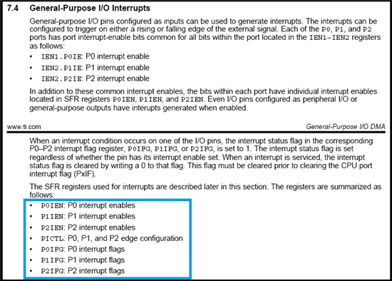
#define HAL_KEY_SW_1_IEN          IEN1  /* CPU interrupt mask register */
#define HAL_KEY_SW_1_ICTL        P0IEN /* Port Interrupt Control register */
#define HAL_KEY_SW_1_ICTLBIT  BV(0) /* P0IEN - P0.0 enable/disable bit */
#define HAL_KEY_SW_1_IENBIT BV(5) /* Mask bit for all of Port_0 */
#define HAL_KEY_SW_1_PXIFG     P0IFG /* Interrupt flag at source */

#define HAL_KEY_SW_2_IEN          IEN1  /* CPU interrupt mask register */
#define HAL_KEY_SW_2_ICTL        P0IEN /* Port Interrupt Control register */
#define HAL_KEY_SW_2_ICTLBIT  BV(1) /* P0IEN - P0.1 enable/disable bit */
#define HAL_KEY_SW_2_IENBIT BV(5) /* Mask bit for all of Port_0 */
#define HAL_KEY_SW_2_PXIFG     P0IFG /* Interrupt flag at source */

thanks in advance, 
~LD
  • According to the keyfob schematic, the keyfob buttons are on P0_0 & P0_1. The Port 0 interrupt enable bit P0IE is at bit index 5 (or bit 6) of the IEN1 register (refer to CC2540 user guide), hence the setting of IEN1 to a value of BV(5) to enable P0 interrupts.

  • Consider IEN as a general interrupt switch. By switching the bit you mention, the WHOLE port 0 is affected.

  • dumb question,,, why in particular "5"... why not BV(0)  or BV(1) ?  are you saying that any value from 0~7 will work just fine?

  • I'm REMEMBERING but I think BV was a C macro.

    BV(5) is a way to indicate the 5 Less Significant Bit individually.

    Since the IEN1 is structured in the following manner (TI designed this way):

    IEN1 (0xB8) – Interrupt Enable 1
    Bit Name Reset R/W Description
    7:6 – 00 R0 Reserved. Read as 0
    5 P0IE 0 R/W Port 0 interrupt enable
    4 T4IE 0 R/W Timer 4 interrupt enable
    3 T3IE 0 R/W Timer 3 interrupt enable
    2 T2IE 0 R/W Timer 2 interrupt enable
    1 T1IE 0 R/W Timer 1 interrupt enable
    0 DMAIE 0 R/W DMA transfer interrupt enable

    If you employ BV(2) for example, you are going to disable the timer2 interrupt :) IEN is an interrupt register that allows to disable whole things at once.
  • Thanks for answer.  I see the definitions in file ioCC2540.h. hence Port 0 interrupt is set at bit 5 of IEN1 reg...

    Does that mean I can not set interrupt on Port 1 because I do not see P1IE definitions in ioCC2540.h.  My application needs to have interrupt on P1_0?

    ~LD

  • At first it was hard for me to find this document.

    I guess it will help you a lot :)

    6404.cc253x_2540x_um.pdf

  • P1IE is IEN2 bit4. Do you have the CC2530/40 user guide?

    1960865 said:

    Thanks for answer.  I see the definitions in file ioCC2540.h. hence Port 0 interrupt is set at bit 5 of IEN1 reg...

    Does that mean I can not set interrupt on Port 1 because I do not see P1IE definitions in ioCC2540.h.  My application needs to have interrupt on P1_0?

    ~LD

  • Michael

    I was under the impression that if "P0IE" is an interrupt for Port 0, then I should be able to see P1IE interrupt for port 1.  The IEN1 that Kazola and you pointed out has bit 5 for Port0 but I dont see for port 1 or port 2.  The manual I am using is "swru191c".

    SFRBIT( IEN1    ,  0xB8, _IEN17, _IEN16, P0IE, T4IE, T3IE, T2IE, T1IE, DMAIE )


    thanks
    ~LD
    
    
  • I will try that and see... thanks for your help.. I am bouncing back n forth from topic to topic and confusing myself... 

  • Check IEN2 or IEN0, I do not remember which was.

  • As per my previous post it is in the IEN2 register. Note that IEN0, IEN1 & IEN2 do not correspond to port 0,1,2 respectively. Have another look at the user guide (page 43 of SWRU191B).

    Note that many of the system register bits are not mapped in the ioCC2540.h file, you have to either create it yourself the same way as other registers

    SFRBIT( IEN2    ,  0x9A, _IEN27, _IEN26, _IEN25, P1IE..............

    or simply write the value e.g.

    #define SET_P1IE IEN2 |= (1 << 4)

    #define CLR_P1IE IEN2 &= ~(1 << 4)

    As for the BV(5), BV(x) is a macro equivalent to 1 << x, so BV(5) = 1 << 5 = 0x20 which sets bit 5 but clears all other bits

  • Mike

    Thanks for your inputs. I do see the problem now.  I was searching for the keywords based on the attached file..

    <swru191b.pdf pages 78 & 79>

    I assumed that when a file is named "ioCC2540.h"; it should contain the entire hardware map or at least indicate in the file itself. 

    ~LD