Because of the holidays, TI E2E™ design support forum responses will be delayed from Dec. 25 through Jan. 2. Thank you for your patience.

This thread has been locked.

If you have a related question, please click the "Ask a related question" button in the top right corner. The newly created question will be automatically linked to this question.

IFA (Inverted F Antenna) eagle liberary

Other Parts Discussed in Thread: CC2540, CC2511

Hi

I want to add to a pcb the IFA antenat so it will work with the cc2540 (the same as in the CC2540_MiniDK, any chance you

will put the CC2540_MiniDK in tideals)

after reading http://www.ti.com/lit/an/swra117d/swra117d.pdf I understand it should be designed very carefully

is therer all ready made eagle liberary for this antena (or even better for the entire  CC2540_MiniDK)?

can I find the antena as eagle part?

if not is there any way to convert the DXF or gerber files you mentionsd in the pdf to Eagle format?

thanks

  • Hi Natanel,

    I'm not sure if this is what you are looking for,

    but the CC2540 Keyfob and dongle reference designs

    can be found here, respectively:

    http://www.ti.com/tool/cc2540keyfob-rd

    http://www.ti.com/tool/cc2540usb-rd

    Both designs made in cadstar, so I don't know if it can be imported to eagle.

  • thanks

    I already found it, I need a way to convert it or find existing antenna library for eagle.

    so I can easily design and send it to batch PCB 

  • Hi,

    Well, I'm not sure the PCB antenna is a component there. I've used AN043

    to draw the same type of antenna, may be you'll find it useful.

    Here's a link: http://www.ti.com/lit/an/swra117d/swra117d.pdf

  • Hi Igor,

    as you can see I allready found this link (see my first post) 

    I am very new to pcb desgine and afraid that this antena desgin will be my bottleneck

    I hoped to find it as simple to add component in eagle.

    or thought using ceramic chip antenna like this http://www.sparkfun.com/products/144

    but again ceramic chip antena as it set of rules.

    in your opinion which one is easy to handle? (let call it more "mistake friendly")

    if you can ,please, add your openion to my other post http://e2e.ti.com/support/low_power_rf/f/538/t/195111.aspx 

    what make me worried are lines like this from the ANO43 "It is also recommended to use the same thickness and type of PCB material"

    it look like that each line in the PCB can harm the antenna functionality, and again I am not really export in this

    thanks

  • Hey,

    natanel said:
    as you can see I allready found this link (see my first post) 

    I've managed to miss it :) 

    natanel said:
    in your opinion which one is easy to handle? (let call it more "mistake friendly")

    I think the IFA.

    What PCB formats supported by eagle? My be I can help you by converting it.

    Another question, what design you prefer, with discrete components or with Balun?

    natanel said:
    "It is also recommended to use the same thickness and type of PCB material

    The same thickness is pretty easy to follow, 1.4mil (1OZ) is a pretty standard track thickness

    when manufacturing PCB. Regarding PCB material, well, you can decide about it a little bit later

    (like before sending the PCB to manufacturer)

  • Hi

    In eagle you create *.sch and *.brd files, than you can run script that convert it  to gerber files under some rules (GBL,GBO,GBS,GTL,GTO,GTS,GTP,drill.txt ) and from there sending it to batchPCB, few week later you will get  in mail your designed PCB

    it is quit popular program  in the hobbiy world (see sparkfun site for example)

    it also have an editor to create component with symbol (to use in *.sch) and package (to use in *.brd)

    I thought of using pre defined antenna component (at least as component) and just copy/past it to any project needed

    also I prefer the balun as it will force less desgin mistakes

    thanks

  • Hi,

    I'm not sure if the conversion gone well, check the attached file.

    If you can see some information there, please make a screenshot

    of the board, and post me back so I could verify it somehow

    8267.CC2540_USB_Dongle.brd

  • Hi,

    the brd files you sent is not eagle format, can not use it

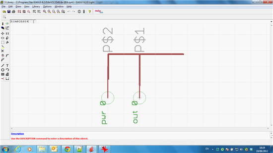
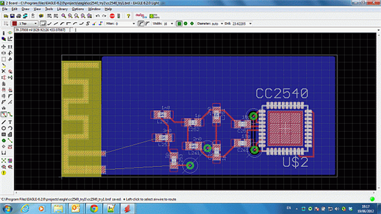
    I created a component named IFA (at least tried) using the ANO43 description

    few general design question

    - what are the deimention for the ground plate?

    - is it connected to real ground or just a plate?

    - is the ground plate can be the same ground of other components?

    - what is the size of the via to the ground plate?

    - the "Figure 1: CC2511 USB Dongle" in ANO43 show special size wire connected to the L253

    and all the balun components are connected in special order. is it importan? is there some document describing it?

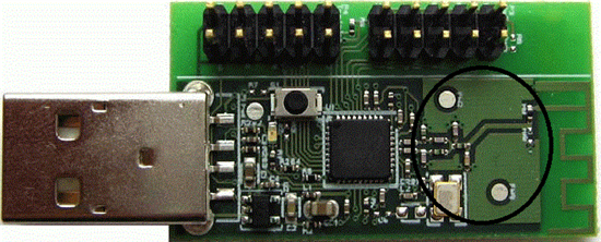
    - the "Figure 1: CC2511 USB Dongle" in ANO43 show special plate connected between the antenna and the balun ( black circle in attached image).

    is it the ground plate of the antenna?

    is it something else?

    I have also some eagle design questions, I will post them in eagle forum

    thanks

  • Hi Igor

    can you help with my above post?

    thanks

  • Hi Natanel,

    Sorry for the late reply, I'm too busy right now. I'll try to write you an answer tomorrow, Ok?

  • Hi Natanel,

    The picture of your antenna looks correct.

    The ground plane should be as big as possible, if you look at the USB dongle reference design you will see that layer 2 is used entierly for ground. I guess you are making a 2-layer board. In that case you should use the top layer for as much as possible of the routing, and fill as much as possible of the bottom layer with ground plane. Do remember to follow the layout of the reference designs closely and do also remember to put vias in the ground pad of the chip (center pad, EPG).

    Antenna ground is the same as "regular" ground.

    The size of the via at the antenna ground connection is not that important. You should however use plenty of vias to connect ground on the top layer with ground on the bottom layer.

    The are you have encircled is just ground plane on the top layer.

    You can also have a look at the CC2544 USB reference design for a more compact design.

    /Fredrik

    The order of the balun components are very important. So is the layout. Follow the reference desing closely.

  • hi igor
    i too need eagle file for inverted f anteena .i got dxf for that i am converting to brd but size is not accurate.can you please help
  • Hi,

    I'm not at the office till Monday. I'll see what I can do to help you out when I'm back.