This thread has been locked.

If you have a related question, please click the "Ask a related question" button in the top right corner. The newly created question will be automatically linked to this question.

S-PVQFN-N76 Footprint for the CC2564

Clarification needed for package dimension.

Below a marked up copy of Fig 16 from the TI QFN PCB Guidelines doc (SWRA420), which indicates dimensions A, B and C – these have been inferred from the Package Dimensions (Fig 15).
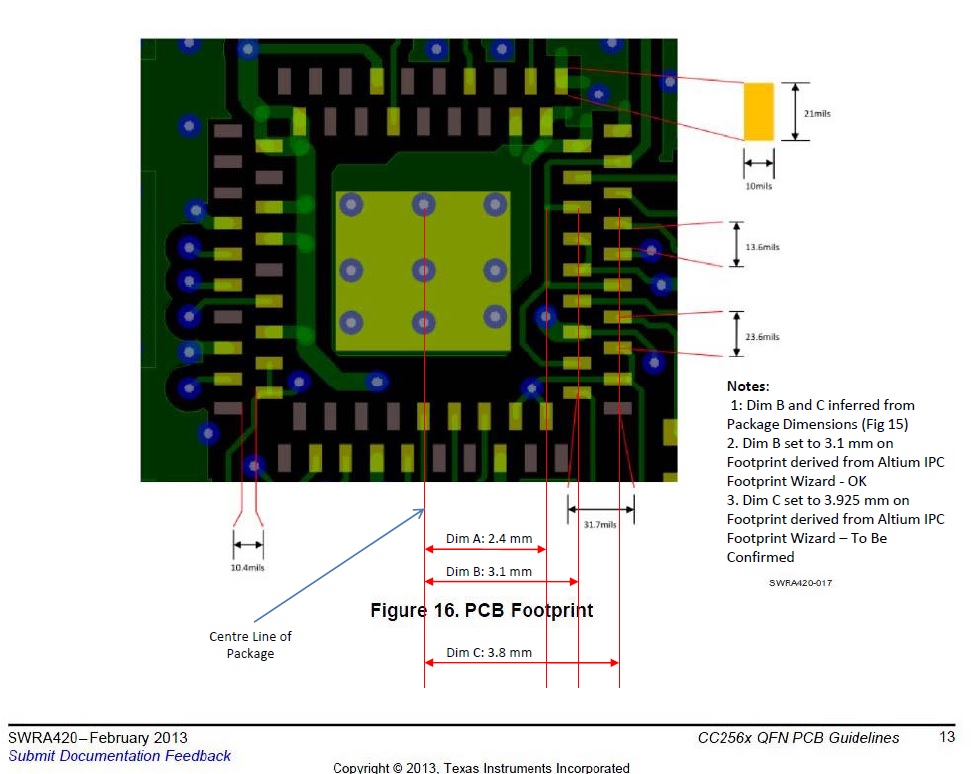
Altium IPC Footprint Wizard was used to generate a Footprint for this part with correspondence on dimensions A and B, but contention on dimension C – the Altium IPC Footprint Wizard indicates that dimension C should be set to 3.925 mm, versus a Package derived value of 3.8 mm. I believe the 3.925 mm dimension is correct for actual assembly of this part - could you please confirm?

  • Did anyone get clarification on this footprint. The drawings for the package do seem to lack dimensions across the device for pad centres?

    My calculations (which make the assumption the component pads are 0.4mm (0.5max ~ 0.3min), would give the centres as 3.6mm (You Dim C), and 2.9mm ( Dim B).

    TI - please create a new Mechanical Drawing or reference PAD layout with full dimensions applied ;-)

  • Hi Chee-Boom Lim,

    Your measurements of Dim A (2.4mm), Dim B (3.1mm) and Dim C (3.8mm) are correct with respect to the pads on the QFN chip.

    Now, the landing pattern (PCB footprint) would be exactly the same if a 1:1 ratio is kept between the QFN pads size and the PCB landing pads size. In this case, the external QFN pads are non-pullback pads extending to the edge of the package and thus we recommend a larger PCB landing pad extending towards the outside of the package for better solderability. Therefore, Dim C will be greater than 3.8mm and it will depend on how large the landing pad size is. Note that Dim B should remain the same since the internal pads are pullback pads.

    I hope it is clear now.

    ~Miguel
  • Rob,

    Please refer to the last post on this thread and let me know if it makes sense now. We will note an action item on our side to better explain this landing pattern on our CC256X QFN PCB Guideline documents.

    BTW, I don't understand how you came up with Dim C = 3.6mm and Dim B = 2.9mm.

    Miguel
  • Hi Miguel,

    Actually didn't use this device in the end, as at the time the footprint was too risky - such a long time back I can't remember much about this now.

    Regards

    Rob

  • Ok. I understand. Let us know if you need further clarification.

    ~Miguel