This thread has been locked.

If you have a related question, please click the "Ask a related question" button in the top right corner. The newly created question will be automatically linked to this question.

CC2541 P0 function block diagram

Other Parts Discussed in Thread: CC2541

Hi :

Can anybody tell me about the CC2541 IO Port0 functional block diagram .By the spec I found the CC2541 is in 8051-core.

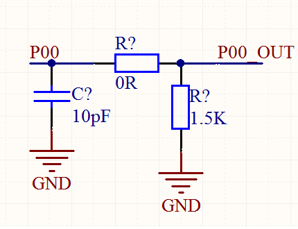
If I configure the P0 with PullUp ( by the spec ,I found the PullUp resistor is 20K ), then I connect a 1.5K resistor to gound ,

  the sch picture like this, then I  set  P0 = 0xFF, what about  the logic level  of P00_OUT and the P00_OUT Voltage is ?

thanks!

  • Hello R,
    internal pullup configured in P0INP is only used for pins configured as input. You need to configure your pin as an output. For example if you want to set P0.1 as output high you need to do the following:

    P0DIR |= 0x02;
    P0_1 = 1;

    Then the output level will be close to VDD. In your case if you set P0 = 0xFF you basically are setting P0.0, P0.1, P0.2 etc... all to 1. You can access a single pin directly instead.
  • Hi:

    Thanks for your reply !

    I see ! 

    I configure the pin as an output . the internal pullup is not used !