This thread has been locked.

If you have a related question, please click the "Ask a related question" button in the top right corner. The newly created question will be automatically linked to this question.

cc2540 problems

Other Parts Discussed in Thread: CC2540, CC2530

Hi everyone,

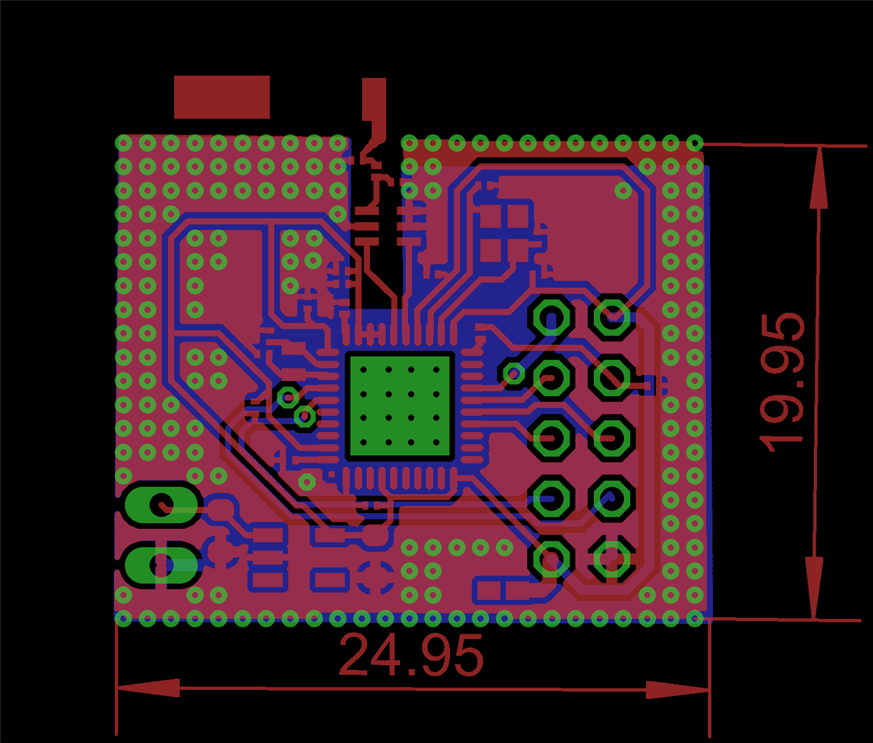
I am working on a design with cc2540, but I dont know if the layout is correct or not, because I have manufactured a previous board (with another components) and it didn't work fine due to layout mistakes, I am worried about this design, I don't want to make the same mistakes.

I attach the layout image, I will add the GND drills in the near of Antenna sections, but I am going to change some external connections, and I haven't put it in this moment:


Best 

  • Since CC254x is for BLE, I would suggest you posting this in Bluetooth® Low Energy Forum.

  • Hi,
    I looked at the picture and have some comments. For a full review, please provide gerber files. For layout recommendations, you can also look under the layout section of the processors.wiki.ti.com/.../CC26xx_HW_Checklist. This is for the CC26xx, but also valid for CC254x (except the DCDC part). The decoupling is not optimal. The order for the power decoupling should be VDD to capacitor to chip VDD pin. There should be a solid GND plane between the decoupling GND vias and GND vias underneath the chip. The decoupling capacitors must be close to the pin it is to decouple. Avoid if possible routing directly underneath the crystal and crystal comp. For the balun, the comp should be placed a bit closer to the RF pins. It is important to keep the balun part as symmetrical as possible. Why do you use some 0201 comp in the balun, it does not appear to save you much space? What is the dotted line? Do you have GND planes on the top layer as well (recommended). I also recommend adding place holders for antenna matching components. I would rotate the shunt filter comp 180 degrees.
  • Thanks for your quick response.

    Regarding to your statement: "The order for the power decoupling should be VDD to capacitor to chip VDD pin", does it mean that I should connect the VDD to the capacitor and the capacitor to the chip VDD pin, or VDD to capacitor and VDD pin simoultaneously?

    I have another question, I would like to use a SMD chip antenna, Can I use any smd Antenna with 50 Ohm? There are any recommended component?

    Thanks in advance

    Regards

    Here I attach an updated schematics.

  • To your question regarding decoupling first, take a look at processors.wiki.ti.com/.../CC26xx_HW_training_Layout_Considerations.pdf (disregard the CC26xx and DCDC specific comments) slide 3 and 7 in particular, these will illustrate what I was trying to say. This still needs work on your design. Also, all RF comp should have separate GND vias and in general more vias connecting the two GND layers. The GND layer on layer 2 should also include the area underneath the chip

    If keeping the PCB antenna, take a look at www.ti.com/.../swra117d.pdf for proper layout ( you can not have GND around or underneath the antenna, I recommend also moving the routing going around the antenna). Yes you can use a SMD chip antenna instead, but I would still recommend place holders for antenna mathcing components. The are many vendors for such antenna with good performance and the different vendors all have their own guidelines on layout and matching to 50 ohm. We have several designs with chip antennas, see for instant www.ti.com/.../CC2541-POSTAGE-STAMP-RD. The antenna selection guide can help to better explain different antenna parameters and advantages with different kinds of antennas, see www.ti.com/.../swra161b.pdf.
  • Hi CHS, Thanks for your reply.

    I have solved few mistakes (I think), I am going to use the 2450BM15A0002 balun, and the associed Antenna, I have a question about the line between the antenna and the balun, the specifications recommends draw a line with 50 Ohm impedance, but I don't know to ensure a line with this characteristic.

    This is the last update:

    Thanks a lot.

    Andrés

  • You still need GND under the CC2540 chip. Also the balun should be closer to the RF pins on the CC2540.
  • Hello CHS,

    Thanks for your answer, it was very useful. I have changed those features, I have routed the GND to underneath chip, and put closely the balun, but I have read the antenna wire must have impedance 50 Ohm, Have I to make a determinate route to antenna, or this information is about the antenna value?

    Thanks a lot.

    Andrés.

  • If the length of the trace between the antenna and balun is longer than 1/10 of the wavelength, it will be like a transmission line and you will need to calculate the trace width. In your design it looks quite short though, so I would not be to concerned. There are several good online transmission line calculators if you want to try, for instant
    www.awrcorp.com/.../tx-line-transmission-line-calculator
    Typically you can make co-planar waveguides with ground with 50 ohm impedance with 0.15 - 0.2 mm clearance to surrounding ground plance.
  • Hi CHS,

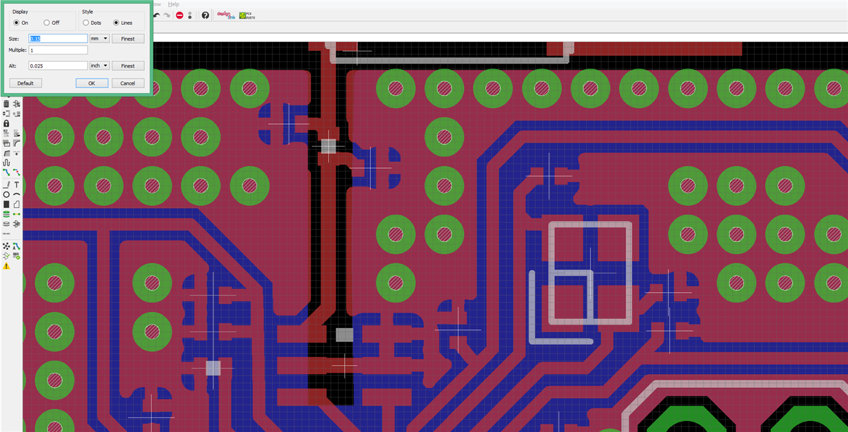
    I have modified the trace between the antenna and balun, I have set 0.15mm more or less of clearance (like the picture). Is this ok? or not?

    Thanks a lot.

    Andrés

  • Two things I just notice though, sorry for not pointing them out earlier. You should have GND underneath the RF path and balun to the antenna as well. And the balun should have better GND (try to add a via under the chip balun and to the side of the balun. I found the reference design for this balun for the CC2530 (different radio, but still a good ref design to copy), this is attached. CC2530_JTI_balun_ref_design_swrr065.zip