This thread has been locked.

If you have a related question, please click the "Ask a related question" button in the top right corner. The newly created question will be automatically linked to this question.

CC2541 CC2590 Antenna Design

Other Parts Discussed in Thread: CC2541, CC2590, CC2591, CC2592

Hello,

We are designing a product with the CC2541+CC2590

For best performance the Application Note AN120 recommends following the reference PCB layout closely.

Given size constants of our design, will it degrade performance if the CC2590 antenna trace and parts connected to Pin 11 are not in a not straight line as shown in the reference design swrr116 but the PCB trace and parts connected to Pin 11 are rotated 90 degrees downward? 

Also pin 1 on the CC2590 is designated as No Connect or (NC) if so way in the reference designed tied to the supply voltage and decoupled?

Thanks,

Best Regards,

Blair Fredericks

  • Hi Blair,

    It should be ok to make a 90 degree bend in the RF path, but make sure all the distances between components are the same as in the reference design. It is probably better to make the turn a few components out from CC2590 to avoid getting a long trace between the CC2590 and the first filter component.

    Pin 1 is connected to VDD to be pin compatible with the CC2591 for internal testing. In your design you can remove this connection and associated components.

    Cheers,
    Fredrik

  • Hello Fredrik,

    Thanks for your advise.

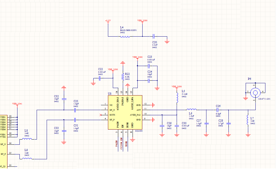
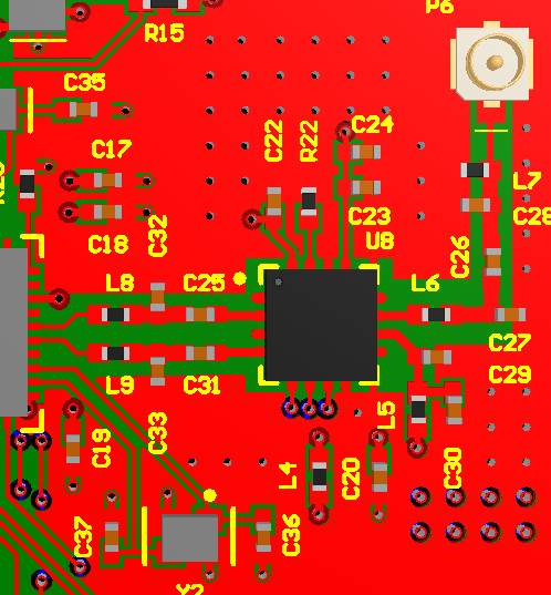
    Could you please advise regarding my layout and the use of a UFL connector, images are below.

    Schematic Part

    Layout 3D View

    Top Layer

    Layer View

    Any input regarding this layout would be greatly appreciated!

    Thank you,

    Best Regards,

    Blair Fredericks

  • Hi Blair,

    The layout looks good. I would expect this to work very well.

    Cheers,
    Fredrik

  • Hello Fredrik

    I have prototype built and it is not working as expected.

    I have a few question?

    Where can I purchase the CC2541-CC2590EMK?
    At least that would give me some kinda base line.

    I am using the TI Packet Sniffer I am seeing packets with at best -30 dbm is this accurate?
    I would expect to be seeing allot better then that, like 10 dbm.
    I lose connect with any distances greater then 2 meters I assume this because of the LNA not working or being controlled correctly.

    I have notice in allot of other designs they have either an inductor or 1K resistor in series with the control lines HGM, EN, PA_EN
    I did not include these in my design, how critical are these?
    Yes, there seems to be allot of noise on these lines, probably why this is done, right?

    I also have notice in allot of designs they follow the reference design exactly and connect Pin 1 of the CC2590 to power?
    I did not do this in my design.

    Would you recommend going to the CC2592?
    It would seems less complicated and the pin out is optimized and is more suitable for PCB layout.
    I release also that IC provides a stronger RF signal that is not BT compliant.

    Thanks,

    Best,

    Blair
  • Hi Blair,

    Unfortunately, the CC2541-CC2590EM is a reference design only, it is not available as a kit.

    Radiated measurements will not be accurate in measuring output power. The only way to do this properly is with conducted measurements. The range test though is valid, and if you lose connection beyond 2 meters, there is obviously something wrong.

    The series components on the control lines are not critical for the RF performance, they are used for noise filtering/reduction.

    CC2590 does not require anything to be connected to pin 1. The pin is true NC, meaning it is not connected internally in the package. The reason a few reference designs still have this pin connected is to be compatible with the CC2591.

    I do not think going to CC2592 is the best start to solve the issues you have. I would rather start with connecting the board to a spectrum analyzer and control it from SmartRF Studio to take SW out of the equation. Are the control signals asserted correctly with SmartRF Studio? Is the output power as expected? If so, run the BLE stack and the HCI TX test transmit (or whatever it is called) command. Do you see the same as with Studio?

    Cheers,
    Fredrik
  • Hello Fredrik,

    Thanks for your reply.

    I setup and RF Studio and did some testing, thanks I did not even consider that.

    I tested one my boards to make sure the ground plane was indeed on layer 2 and not swapped.

    I do include Fabrication Instructions with my boards.

    The Prepeg seemed very thin, so I got thinking I should see how my stack up compares to what is recommended.

    This is the recommended Stack Up

    PCB description: 4 layer PCB 1.6mm

    Copper 1: 35 mm

    Dielectric 1-2: 0.35 mm (e.g. 2x Prepreg 7628 AT05 47% Resin)

    Copper 2: 18 mm

    Dielectric 2-3: 0.76 mm (4 x 7628M 43% Resin)

    Copper 3: 18 mm

    Dielectric 3-4: 0.35 mm (e.g. 2x Prepreg 7628 AT05 47% Resin)

    Copper 4: 35 mm

    DE104iML or equivalent substrate (Resin contents around 45%, which gives Er=4.42 at 2.4GHz, TanD=0.016)

    This is my board stack up.

    PCB description: 4 layer PCB 1.6mm

    Copper 1: 35 mm

    Dielectric 0.2 mm

    Copper 2: 18 mm

    Dielectric 1.1 mm

    Copper 3: 18 mm

    Dielectric 0.2 mm

    Copper 4: 35 mm

    Clearly the dielectric layers are not the same!

    How big of a impact would this have?

    It would seem I have ruled out everything.

    It would seem the board stack up is the problem?

    If so, well time to spin a new board.

    Thanks,

    Best Regards,

    Blair

  • HI Blair,

    That stack-up will definitely affect the performance. Before ordering new boards, I would still do some more debugging.

    - What is the conducted output power?
    - Are the control signals toggling correctly?

    BR,
    Fredrik
  • Hello Fredrik,

    When using RF Studio the control lines for TX are doing what I would expected.
    HGM goes High and PA_EN goes high continuously.
    However with RX with the Range Extender set to CC2590 and High Gain Mode set.
    The control line EN or LNA_EN goes high, but just like in the BLE Stack with POWER_SAVING not defined, the HGM still never goes high?

    My understanding this has nothing to do with BLE Stack the controls lines are controlled by CEBAL.
    Given that, it is kinda hard to conduct a complete test if the LNA is never in High Gain.
    At this point I do not have a Spectrum Analyzer, so the only output power I can see is what any software is showing me.
    I did do some TX testing with RF Studio and using Packet Sniffer, I would adjust the TX power down and the RSSI would go down.
    Still I never see anything better then -29 dbm.

    At this point I just know the one and only one thing I did not do correctly is getting the board fabricated with the correct PCB Stack-up?
    By process of elimination, the PCB Stack-up seems to be the problem.
    Clearly the Stack-up is wrong, however should I be getting the results I am getting with this PCB Stack-up?
    Also not sure why, the RX control lines are not working correctly?

    If you have any further suggestions I would be very grateful.

    Regards,

    Blair
  • First just a comment on the stack-up; on our reference design we have the following stack-up for layer 1 and 2 (the most important part)
    Copper 1 35 um
    Dielectric 1-2 0.175 mm (e.g. 1x Prepreg 7628 AT05 47% Resin)
    Copper 2 18 um
    so it is quite similar to yours ( you have 0.2 mm for dielectric between layer 1 and 2). Thus I do not believe this affect your performance that much.

    Not sure I completely understand what you are measuring when using Smart RF studio, do you see an increase in the output power? What you should measure on the control signals are: for TX PAEN high, HGM does not matter, EN low. For RX, PAEN low, HGM and EN high. Is this what you are seeing? Are you using the same pins to control the CC2590 as in our ref design?

    I understand that you do not have a spectrum analyzer which makes this hard to debug. Is the current consumption as expected? What output power (or RSSI on the sniffer) do you measure if you use a CC2541 EM stand alone compared to your design with the CC2590 on the board?
  • Hello,

    I have to agree that the PCB Stack-up should not degrade the performance like what I am seeing.

    When using Smart RF Studio and doing a continuous RX or Packet with High Gain Selected and the Range Extender CC2590.

    I am seeing  EN HIGH or pin 6 on the CC2590.

    I am seeing  HGM LOW or pin 7 on the CC2590, that is with High Gain Enabled, i hope that is clear.

    Yes I am using the same control pins as in your reference design, my schematic is included.

    I am getting OK distance with Transmit.

    You must have a few CC2541-CC2590EM boards around, hook them up, run some test with Smart RF Studio.

    Do you see what you think you should be seeing the control lines?

    Are you getting the performance you expect?

    The real problem is receiver sensitivity.

    I have a Spectrum Analyzer on the way should be here in a few days.

    Then I can measure the output power.

    Regards,

    Blair

  • You are correct, I also see the HGM pin low in RX when using SmartRF studio. I have reported this issue to the tools team. For test, what happens if you hardwire the HGM to high (cut the line and connect to VDD) (if you have enough boards)?
  • Hello Charlotte,

    Thank you very much for looking into this.

    Also I am not just seeing this in Smart RF Studio.
    I am having similar control line issues in with the BLE Stack when not defining POWER_SAVING, I mentioned this in the post below.

    e2e.ti.com/.../1654036

    I tied HGM to VDD and I still only get about 4 meters.

    Seems regardless of these control issues I have uncovered, I still am have RF receiver sensitivity issues?

    Thanks,

    Blair
  • How have you verified the TX performance? What are the current consumption in the different modes? 4 m is definitively not correct, so something is very wrong. What range do you get if you use the CC2541EM as receiver? Have you tested several boards?
  • Hello,

    There where allot of issues with my first board, for one the parts supplier provided the wrong value or parts.

    I have since built 2 new boards I am getting much better results and things are working not to bad.
    I am getting indoors around 20 meters, I have not tested anything further at this point.

    I ran some test with RF Studio, I set the TX to continuous mode, the range extender to CC2590, and the power output to 10dbm.
    I have measured the output power directly connected with a spectrum analyzer and I am getting -2dbm.
    I also measured the power over the air and I am getting about -20dbm at about 1 meter.
    I also measured the current consumption of the CC2590 I am getting between 18 and 23.8 mA depending on the orientation
    UFL connector and the antenna. That from what I understand is about right for current draw.

    So my question is if I get some boards made with the correct stack up can I expect to see around 10dbm?
    What are the test conditions under which this output power is expected?

    I wanted to change my design so that I make a 90 degree turn right at the antenna pin, not a few parts in.
    I have see I few designs, they are doing this?

    www.elance.com/.../

    www.aliexpress.com/.../2021950192.html

    Thanks for all your help,

    Regards,

    Blair
  • These are conducted measurements or radiated? And you have verified the control signals? the current consumption you state is for the CC2590 alone I assume, because then they make sense. How are you making your boards, are you mounting all components yourself?

    I do not believe this is caused by the change in stack up (200 um vs 175 um) nor the 90 degree, when you checked the components, did you verify the comp for the VDD decoupling and RBIAS for the CC2590 part as well? If you look at the output signal with a signal analyzer with a large span, do you see any unexpected spurious?