This thread has been locked.

If you have a related question, please click the "Ask a related question" button in the top right corner. The newly created question will be automatically linked to this question.

Bricked CC2650

Other Parts Discussed in Thread: CC2650, CC1310, UNIFLASH

I am using a SmartRF06 board connected via JTAG to our custom board. I have been successfully using CCS to program and debug with this setup for a couple of months, but now the CC2650 appears to be bricked.

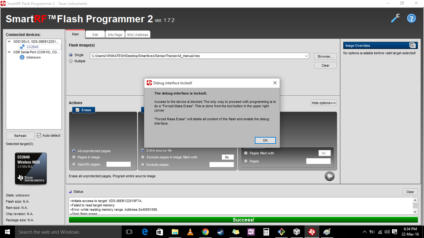
When I try using Smart Flash Programmer 2 v1.7.1 to do a Forced Mass Erase, it says that it completed successfully but if I then try to program the device it fails. I have looked at similar posts in this forum but can't find anything that works. Any ideas how to get this chip going again?

Smart Flash Programmer logs:
>>>> Forced Mass Erase

>Initiate access to target: XDS-06EB12202209A.
>Failed to read target memory.
>Error while reading memory range. Address 0x40091090.
>Start flash erase ...
>Erase finished successfully.
>Reset target ...
>Reset of target successfull.

>>>> Erase/Program/Verify with image file

>Initiate access to target: XDS-06EB12202209A.
>Failed to read target memory.
>Error while reading memory range. Address 0x40091090.
>Debug interface is locked. Aborting action. Only forced mass erase is possible.
>Reset target ...
>Reset of target successfull.

  • Check if your CC2650 is well powered.
  • Supply voltage looks fine at 3.7v. I have tried manually resetting it, no luck so far.
  • Do you have another CC2650 to test? I suggest you using another CC2650 to test if this is an issue on CC2650 or it is an issue of your SmartRF06 board.
  • yes I just tried another board and that one programs ok. Is it possible to brick a CC2650 via software by overwriting the CCFG etc or should it always be recoverable using Forced Mass Erase?
  • Hi Martin,

    If you overwrite CCFG with only zeroes you will effectively have locked yourself out since all JTAG DAPs/TAPs are disabled, bootloader is disabled and mass erase is disabled. See the memory map for an overview of which fields are written to zero in this case. Path in the 2.1 SDK would typically be:
    C:/ti/tirtos_simplelink_2_13_00_06/products/cc26xxware_2_21_01_15600/doc/register_descriptions/CPU_MMAP/CCFG.html

    Regards,
    Svend
  • Hi Svend,

    I am also facing the same problem as described but how do I overwrite CCFG with the previous config instead of Zeroes. Please suggest some solutions ASAP.

    Regards,

    Venkat

  • Are you able to do a mass erase with flash programmer 2?
  • Yeah when a mass erase is done it shows that it is successful.

    Regards,
    Venkat
  • I have done the same thing (Erase all unprotected pages) and have the exact scenario described in this thread (mass erase claims success, but still the device is unreachable). If anyone has a solution it would be very very much appreciated.

  • What's the flash programmer version you have?
  • SmartRF flash programmer 2 - version 1.7.2

  • I would suggest you to ask for replacement from www.ti.com/.../faq-returns-and-refunds.page
  • Can you show me the ccfg file you used to program the device? After you program the device, did you do a reset before connecting to flash programmer? Was there pop-up screen said device is locked?
  • Hi,

    CCFG region got corrupted due to a bug in OAD, CCS is unable to access the Core through JTAG. 

    Can you please let me know how to recover the JTAG connectivity?

  • Moving to Bluetooth Smart forum

    Regards,
    Gigi Joseph.
  • Can you try to use flash programmer to see if you can gain access to the device? If yes, try to use mass erase to recover the device
    You can download flash programmer 2 here :
    software-dl.ti.com/.../self_cert_export.html
  • I tried "Forced Mass erase" option using Flash programmer 2, but internal flash is actually un-erased.

    I could see that program residing in CC2650 is able to advertise over BLE.
  • The ccfg file is given below, yes I did a reset before connecting to flash programmer and I don't remember seeing a pop-up screen which said device is locked.


    /******************************************************************************
    * Filename: ccfg.c
    * Revised: $Date: 2015-03-20 14:44:57 +0100 (fr, 20 mar 2015) $
    * Revision: $Revision: 15313 $
    *
    * Description: Customer Configuration for CC26xx device family (HW rev 2).
    *
    * Copyright (C) 2014 Texas Instruments Incorporated - http://www.ti.com/
    *
    *
    * Redistribution and use in source and binary forms, with or without
    * modification, are permitted provided that the following conditions
    * are met:
    *
    * Redistributions of source code must retain the above copyright
    * notice, this list of conditions and the following disclaimer.
    *
    * Redistributions in binary form must reproduce the above copyright
    * notice, this list of conditions and the following disclaimer in the
    * documentation and/or other materials provided with the distribution.
    *
    * Neither the name of Texas Instruments Incorporated nor the names of
    * its contributors may be used to endorse or promote products derived
    * from this software without specific prior written permission.
    *
    * THIS SOFTWARE IS PROVIDED BY THE COPYRIGHT HOLDERS AND CONTRIBUTORS
    * "AS IS" AND ANY EXPRESS OR IMPLIED WARRANTIES, INCLUDING, BUT NOT
    * LIMITED TO, THE IMPLIED WARRANTIES OF MERCHANTABILITY AND FITNESS FOR
    * A PARTICULAR PURPOSE ARE DISCLAIMED. IN NO EVENT SHALL THE COPYRIGHT
    * OWNER OR CONTRIBUTORS BE LIABLE FOR ANY DIRECT, INDIRECT, INCIDENTAL,
    * SPECIAL, EXEMPLARY, OR CONSEQUENTIAL DAMAGES (INCLUDING, BUT NOT
    * LIMITED TO, PROCUREMENT OF SUBSTITUTE GOODS OR SERVICES; LOSS OF USE,
    * DATA, OR PROFITS; OR BUSINESS INTERRUPTION) HOWEVER CAUSED AND ON ANY
    * THEORY OF LIABILITY, WHETHER IN CONTRACT, STRICT LIABILITY, OR TORT
    * (INCLUDING NEGLIGENCE OR OTHERWISE) ARISING IN ANY WAY OUT OF THE USE
    * OF THIS SOFTWARE, EVEN IF ADVISED OF THE POSSIBILITY OF SUCH DAMAGE.
    *
    ******************************************************************************/

    #include <stdint.h>
    #include <inc/hw_types.h>
    #include <inc/hw_ccfg.h>
    #include <inc/hw_ccfg_simple_struct.h>

    //*****************************************************************************
    //
    // Introduction
    //
    // This file contains fields used by Boot ROM, startup code, and SW radio
    // stacks to configure chip behavior.
    //
    // Fields are documented in more details in hw_ccfg.h and CCFG.html in
    // DriverLib documentation (doc_overview.html -> CPU Domain Memory Map -> CCFG).
    //
    //*****************************************************************************

    //*****************************************************************************
    //
    // Set the values of the individual bit fields.
    //
    //*****************************************************************************

    //#####################################
    // Alternate DC/DC settings
    //#####################################

    #define SET_CCFG_SIZE_AND_DIS_FLAGS_DIS_ALT_DCDC_SETTING 0x0 // Alternate DC/DC setting enabled
    //#define SET_CCFG_SIZE_AND_DIS_FLAGS_DIS_ALT_DCDC_SETTING 0x1 // Alternate DC/DC setting disabled

    #define SET_CCFG_MODE_CONF_1_ALT_DCDC_VMIN 0x8 // 2.25V

    #define SET_CCFG_MODE_CONF_1_ALT_DCDC_DITHER_EN 0x0 // Disable
    //#define SET_CCFG_MODE_CONF_1_ALT_DCDC_DITHER_EN 0x1 // Enable

    #define SET_CCFG_MODE_CONF_1_ALT_DCDC_IPEAK 0x2 // 39mA

    //#####################################
    // XOSC override settings
    //#####################################

    //#define SET_CCFG_SIZE_AND_DIS_FLAGS_DIS_XOSC_OVR 0x0 // Enable override
    #define SET_CCFG_SIZE_AND_DIS_FLAGS_DIS_XOSC_OVR 0x1 // Disable override

    #define SET_CCFG_MODE_CONF_1_DELTA_IBIAS_INIT 0x0 // Delta = 0

    #define SET_CCFG_MODE_CONF_1_DELTA_IBIAS_OFFSET 0x0 // Delta = 0

    #define SET_CCFG_MODE_CONF_1_XOSC_MAX_START 0x10 // 1600us

    //#####################################
    // Power settings
    //#####################################

    #define SET_CCFG_MODE_CONF_VDDR_TRIM_SLEEP_DELTA 0xF // Signed delta value to apply to the VDDR_TRIM_SLEEP target, minus one

    #define SET_CCFG_MODE_CONF_DCDC_RECHARGE 0x0 // Use the DC/DC during recharge in powerdown
    // #define SET_CCFG_MODE_CONF_DCDC_RECHARGE 0x1 // Do not use the DC/DC during recharge in powerdown

    #define SET_CCFG_MODE_CONF_DCDC_ACTIVE 0x0 // Use the DC/DC during active mode
    // #define SET_CCFG_MODE_CONF_DCDC_ACTIVE 0x1 // Do not use the DC/DC during active mode

    // #define SET_CCFG_MODE_CONF_VDDS_BOD_LEVEL 0x0 // VDDS BOD level is 2.0V
    #define SET_CCFG_MODE_CONF_VDDS_BOD_LEVEL 0x1 // VDDS BOD level is 1.8V (or 1.65V for external regulator mode)

    #define SET_CCFG_MODE_CONF_VDDR_CAP 0x3A // Unsigned 8-bit integer representing the min. decoupling capacitance on VDDR in units of 100nF

    //#####################################
    // Clock settings
    //#####################################

    // #define SET_CCFG_MODE_CONF_SCLK_LF_OPTION 0x0 // LF clock derived from High Frequency XOSC
    // #define SET_CCFG_MODE_CONF_SCLK_LF_OPTION 0x1 // External LF clock
    #define SET_CCFG_MODE_CONF_SCLK_LF_OPTION 0x2 // LF XOSC
    // #define SET_CCFG_MODE_CONF_SCLK_LF_OPTION 0x3 // LF RCOSC

    // #define SET_CCFG_MODE_CONF_XOSC_CAP_MOD 0x0 // Apply cap-array delta
    #define SET_CCFG_MODE_CONF_XOSC_CAP_MOD 0x1 // Don't apply cap-array delta

    #define SET_CCFG_MODE_CONF_XOSC_CAPARRAY_DELTA 0xFF // Signed 8-bit value, directly modifying trimmed XOSC cap-array value

    #define SET_CCFG_EXT_LF_CLK_DIO 0x01 // DIO number if using external LF clock

    #define SET_CCFG_EXT_LF_CLK_RTC_INCREMENT 0x800000 // RTC increment representing the external LF clock frequency

    //#####################################
    // Bootloader settings
    //#####################################

    // #define SET_CCFG_BL_CONFIG_BOOTLOADER_ENABLE 0x00 // Disable
    #define SET_CCFG_BL_CONFIG_BOOTLOADER_ENABLE 0xC5 // Enable

    // #define SET_CCFG_BL_CONFIG_BL_LEVEL 0x0 // Active low
    #define SET_CCFG_BL_CONFIG_BL_LEVEL 0x1 // Active high

    #define SET_CCFG_BL_CONFIG_BL_PIN_NUMBER 0xFF // DIO number for boot loader failure analysis

    // #define SET_CCFG_BL_CONFIG_BL_ENABLE 0xC5 // Enabled
    #define SET_CCFG_BL_CONFIG_BL_ENABLE 0xFF // Disabled

    //#####################################
    // Debug access settings
    //#####################################

    // #define SET_CCFG_CCFG_TI_OPTIONS_TI_FA_ENABLE 0x00 // Disable unlocking of TI FA option.
    #define SET_CCFG_CCFG_TI_OPTIONS_TI_FA_ENABLE 0xC5 // Enable unlocking of TI FA option with the unlock code

    // #define SET_CCFG_CCFG_TAP_DAP_0_CPU_DAP_ENABLE 0x00 // Access disabled
    #define SET_CCFG_CCFG_TAP_DAP_0_CPU_DAP_ENABLE 0xC5 // Access enabled if also enabled in FCFG

    // #define SET_CCFG_CCFG_TAP_DAP_0_PRCM_TAP_ENABLE 0x00 // Access disabled
    #define SET_CCFG_CCFG_TAP_DAP_0_PRCM_TAP_ENABLE 0xC5 // Access enabled if also enabled in FCFG

    // #define SET_CCFG_CCFG_TAP_DAP_0_TEST_TAP_ENABLE 0x00 // Access disabled
    #define SET_CCFG_CCFG_TAP_DAP_0_TEST_TAP_ENABLE 0xC5 // Access enabled if also enabled in FCFG

    // #define SET_CCFG_CCFG_TAP_DAP_1_PBIST2_TAP_ENABLE 0x00 // Access disabled
    #define SET_CCFG_CCFG_TAP_DAP_1_PBIST2_TAP_ENABLE 0xC5 // Access enabled if also enabled in FCFG

    // #define SET_CCFG_CCFG_TAP_DAP_1_PBIST1_TAP_ENABLE 0x00 // Access disabled
    #define SET_CCFG_CCFG_TAP_DAP_1_PBIST1_TAP_ENABLE 0xC5 // Access enabled if also enabled in FCFG

    // #define SET_CCFG_CCFG_TAP_DAP_1_WUC_TAP_ENABLE 0x00 // Access disabled
    #define SET_CCFG_CCFG_TAP_DAP_1_WUC_TAP_ENABLE 0xC5 // Access enabled if also enabled in FCFG

    //#####################################
    // Alternative IEEE 802.15.4 MAC address
    //#####################################
    #define SET_CCFG_IEEE_MAC_0 0xFFFFFFFF // Bits [31:0]
    #define SET_CCFG_IEEE_MAC_1 0xFFFFFFFF // Bits [63:32]

    //#####################################
    // Alternative BLE address
    //#####################################
    #define SET_CCFG_IEEE_BLE_0 0xFFFFFFFF // Bits [31:0]
    #define SET_CCFG_IEEE_BLE_1 0xFFFFFFFF // Bits [63:32]

    //#####################################
    // Flash erase settings
    //#####################################

    // #define SET_CCFG_ERASE_CONF_CHIP_ERASE_DIS_N 0x0 // Any chip erase request detected during boot will be ignored
    #define SET_CCFG_ERASE_CONF_CHIP_ERASE_DIS_N 0x1 // Any chip erase request detected during boot will be performed by the boot FW

    // #define SET_CCFG_ERASE_CONF_BANK_ERASE_DIS_N 0x0 // Disable the boot loader bank erase function
    #define SET_CCFG_ERASE_CONF_BANK_ERASE_DIS_N 0x1 // Enable the boot loader bank erase function

    //#####################################
    // Flash image valid
    //#####################################
    #define SET_CCFG_IMAGE_VALID_CONF_IMAGE_VALID 0x00000000 // Flash image is valid
    //#define SET_CCFG_IMAGE_VALID_CONF_IMAGE_VALID <non-zero> // Flash image is invalid, call bootloader

    //#####################################
    // Flash sector write protection
    //#####################################
    #define SET_CCFG_CCFG_PROT_31_0 0xFFFFFFFF
    #define SET_CCFG_CCFG_PROT_63_32 0xFFFFFFFF
    #define SET_CCFG_CCFG_PROT_95_64 0xFFFFFFFF
    #define SET_CCFG_CCFG_PROT_127_96 0xFFFFFFFF

    //*****************************************************************************
    //
    // CCFG values that should not be modified.
    //
    //*****************************************************************************
    #define SET_CCFG_SIZE_AND_DIS_FLAGS_SIZE_OF_CCFG 0x0058
    #define SET_CCFG_SIZE_AND_DIS_FLAGS_DISABLE_FLAGS 0x3FFF

    #define SET_CCFG_MODE_CONF_VDDR_EXT_LOAD 0x1
    #define SET_CCFG_MODE_CONF_RTC_COMP 0x1
    #define SET_CCFG_MODE_CONF_XOSC_FREQ 0x3
    #define SET_CCFG_MODE_CONF_HF_COMP 0x1

    #define SET_CCFG_VOLT_LOAD_0_VDDR_EXT_TP45 0xFF
    #define SET_CCFG_VOLT_LOAD_0_VDDR_EXT_TP25 0xFF
    #define SET_CCFG_VOLT_LOAD_0_VDDR_EXT_TP5 0xFF
    #define SET_CCFG_VOLT_LOAD_0_VDDR_EXT_TM15 0xFF

    #define SET_CCFG_VOLT_LOAD_1_VDDR_EXT_TP125 0xFF
    #define SET_CCFG_VOLT_LOAD_1_VDDR_EXT_TP105 0xFF
    #define SET_CCFG_VOLT_LOAD_1_VDDR_EXT_TP85 0xFF
    #define SET_CCFG_VOLT_LOAD_1_VDDR_EXT_TP65 0xFF

    #define SET_CCFG_RTC_OFFSET_RTC_COMP_P0 0xFFFF
    #define SET_CCFG_RTC_OFFSET_RTC_COMP_P1 0xFF
    #define SET_CCFG_RTC_OFFSET_RTC_COMP_P2 0xFF

    #define SET_CCFG_FREQ_OFFSET_HF_COMP_P0 0xFFFF
    #define SET_CCFG_FREQ_OFFSET_HF_COMP_P1 0xFF
    #define SET_CCFG_FREQ_OFFSET_HF_COMP_P2 0xFF

    //*****************************************************************************
    //
    // Concatenate bit fields to words.
    // DO NOT EDIT!
    //
    //*****************************************************************************
    #define DEFAULT_CCFG_O_EXT_LF_CLK ( \
    ( ((uint32_t)( SET_CCFG_EXT_LF_CLK_DIO << CCFG_EXT_LF_CLK_DIO_S )) | ~CCFG_EXT_LF_CLK_DIO_M ) & \
    ( ((uint32_t)( SET_CCFG_EXT_LF_CLK_RTC_INCREMENT << CCFG_EXT_LF_CLK_RTC_INCREMENT_S )) | ~CCFG_EXT_LF_CLK_RTC_INCREMENT_M ) )

    #define DEFAULT_CCFG_MODE_CONF_1 ( \
    ( ((uint32_t)( SET_CCFG_MODE_CONF_1_ALT_DCDC_VMIN << CCFG_MODE_CONF_1_ALT_DCDC_VMIN_S )) | ~CCFG_MODE_CONF_1_ALT_DCDC_VMIN_M ) & \
    ( ((uint32_t)( SET_CCFG_MODE_CONF_1_ALT_DCDC_DITHER_EN << CCFG_MODE_CONF_1_ALT_DCDC_DITHER_EN_S )) | ~CCFG_MODE_CONF_1_ALT_DCDC_DITHER_EN_M ) & \
    ( ((uint32_t)( SET_CCFG_MODE_CONF_1_ALT_DCDC_IPEAK << CCFG_MODE_CONF_1_ALT_DCDC_IPEAK_S )) | ~CCFG_MODE_CONF_1_ALT_DCDC_IPEAK_M ) & \
    ( ((uint32_t)( SET_CCFG_MODE_CONF_1_DELTA_IBIAS_INIT << CCFG_MODE_CONF_1_DELTA_IBIAS_INIT_S )) | ~CCFG_MODE_CONF_1_DELTA_IBIAS_INIT_M ) & \
    ( ((uint32_t)( SET_CCFG_MODE_CONF_1_DELTA_IBIAS_OFFSET << CCFG_MODE_CONF_1_DELTA_IBIAS_OFFSET_S )) | ~CCFG_MODE_CONF_1_DELTA_IBIAS_OFFSET_M ) & \
    ( ((uint32_t)( SET_CCFG_MODE_CONF_1_XOSC_MAX_START << CCFG_MODE_CONF_1_XOSC_MAX_START_S )) | ~CCFG_MODE_CONF_1_XOSC_MAX_START_M ) )

    #define DEFAULT_CCFG_SIZE_AND_DIS_FLAGS ( \
    ( ((uint32_t)( SET_CCFG_SIZE_AND_DIS_FLAGS_SIZE_OF_CCFG << CCFG_SIZE_AND_DIS_FLAGS_SIZE_OF_CCFG_S )) | ~CCFG_SIZE_AND_DIS_FLAGS_SIZE_OF_CCFG_M ) & \
    ( ((uint32_t)( SET_CCFG_SIZE_AND_DIS_FLAGS_DISABLE_FLAGS << CCFG_SIZE_AND_DIS_FLAGS_DISABLE_FLAGS_S )) | ~CCFG_SIZE_AND_DIS_FLAGS_DISABLE_FLAGS_M ) & \
    ( ((uint32_t)( SET_CCFG_SIZE_AND_DIS_FLAGS_DIS_ALT_DCDC_SETTING << CCFG_SIZE_AND_DIS_FLAGS_DIS_ALT_DCDC_SETTING_S )) | ~CCFG_SIZE_AND_DIS_FLAGS_DIS_ALT_DCDC_SETTING_M ) & \
    ( ((uint32_t)( SET_CCFG_SIZE_AND_DIS_FLAGS_DIS_XOSC_OVR << CCFG_SIZE_AND_DIS_FLAGS_DIS_XOSC_OVR_S )) | ~CCFG_SIZE_AND_DIS_FLAGS_DIS_XOSC_OVR_M ) )

    #define DEFAULT_CCFG_MODE_CONF ( \
    ( ((uint32_t)( SET_CCFG_MODE_CONF_VDDR_TRIM_SLEEP_DELTA << CCFG_MODE_CONF_VDDR_TRIM_SLEEP_DELTA_S )) | ~CCFG_MODE_CONF_VDDR_TRIM_SLEEP_DELTA_M ) & \
    ( ((uint32_t)( SET_CCFG_MODE_CONF_DCDC_RECHARGE << CCFG_MODE_CONF_DCDC_RECHARGE_S )) | ~CCFG_MODE_CONF_DCDC_RECHARGE_M ) & \
    ( ((uint32_t)( SET_CCFG_MODE_CONF_DCDC_ACTIVE << CCFG_MODE_CONF_DCDC_ACTIVE_S )) | ~CCFG_MODE_CONF_DCDC_ACTIVE_M ) & \
    ( ((uint32_t)( SET_CCFG_MODE_CONF_VDDR_EXT_LOAD << CCFG_MODE_CONF_VDDR_EXT_LOAD_S )) | ~CCFG_MODE_CONF_VDDR_EXT_LOAD_M ) & \
    ( ((uint32_t)( SET_CCFG_MODE_CONF_VDDS_BOD_LEVEL << CCFG_MODE_CONF_VDDS_BOD_LEVEL_S )) | ~CCFG_MODE_CONF_VDDS_BOD_LEVEL_M ) & \
    ( ((uint32_t)( SET_CCFG_MODE_CONF_SCLK_LF_OPTION << CCFG_MODE_CONF_SCLK_LF_OPTION_S )) | ~CCFG_MODE_CONF_SCLK_LF_OPTION_M ) & \
    ( ((uint32_t)( SET_CCFG_MODE_CONF_RTC_COMP << CCFG_MODE_CONF_RTC_COMP_S )) | ~CCFG_MODE_CONF_RTC_COMP_M ) & \
    ( ((uint32_t)( SET_CCFG_MODE_CONF_XOSC_FREQ << CCFG_MODE_CONF_XOSC_FREQ_S )) | ~CCFG_MODE_CONF_XOSC_FREQ_M ) & \
    ( ((uint32_t)( SET_CCFG_MODE_CONF_XOSC_CAP_MOD << CCFG_MODE_CONF_XOSC_CAP_MOD_S )) | ~CCFG_MODE_CONF_XOSC_CAP_MOD_M ) & \
    ( ((uint32_t)( SET_CCFG_MODE_CONF_HF_COMP << CCFG_MODE_CONF_HF_COMP_S )) | ~CCFG_MODE_CONF_HF_COMP_M ) & \
    ( ((uint32_t)( SET_CCFG_MODE_CONF_XOSC_CAPARRAY_DELTA << CCFG_MODE_CONF_XOSC_CAPARRAY_DELTA_S )) | ~CCFG_MODE_CONF_XOSC_CAPARRAY_DELTA_M ) & \
    ( ((uint32_t)( SET_CCFG_MODE_CONF_VDDR_CAP << CCFG_MODE_CONF_VDDR_CAP_S )) | ~CCFG_MODE_CONF_VDDR_CAP_M ) )

    #define DEFAULT_CCFG_VOLT_LOAD_0 ( \
    ( ((uint32_t)( SET_CCFG_VOLT_LOAD_0_VDDR_EXT_TP45 << CCFG_VOLT_LOAD_0_VDDR_EXT_TP45_S )) | ~CCFG_VOLT_LOAD_0_VDDR_EXT_TP45_M ) & \
    ( ((uint32_t)( SET_CCFG_VOLT_LOAD_0_VDDR_EXT_TP25 << CCFG_VOLT_LOAD_0_VDDR_EXT_TP25_S )) | ~CCFG_VOLT_LOAD_0_VDDR_EXT_TP25_M ) & \
    ( ((uint32_t)( SET_CCFG_VOLT_LOAD_0_VDDR_EXT_TP5 << CCFG_VOLT_LOAD_0_VDDR_EXT_TP5_S )) | ~CCFG_VOLT_LOAD_0_VDDR_EXT_TP5_M ) & \
    ( ((uint32_t)( SET_CCFG_VOLT_LOAD_0_VDDR_EXT_TM15 << CCFG_VOLT_LOAD_0_VDDR_EXT_TM15_S )) | ~CCFG_VOLT_LOAD_0_VDDR_EXT_TM15_M ) )

    #define DEFAULT_CCFG_VOLT_LOAD_1 ( \
    ( ((uint32_t)( SET_CCFG_VOLT_LOAD_1_VDDR_EXT_TP125 << CCFG_VOLT_LOAD_1_VDDR_EXT_TP125_S )) | ~CCFG_VOLT_LOAD_1_VDDR_EXT_TP125_M ) & \
    ( ((uint32_t)( SET_CCFG_VOLT_LOAD_1_VDDR_EXT_TP105 << CCFG_VOLT_LOAD_1_VDDR_EXT_TP105_S )) | ~CCFG_VOLT_LOAD_1_VDDR_EXT_TP105_M ) & \
    ( ((uint32_t)( SET_CCFG_VOLT_LOAD_1_VDDR_EXT_TP85 << CCFG_VOLT_LOAD_1_VDDR_EXT_TP85_S )) | ~CCFG_VOLT_LOAD_1_VDDR_EXT_TP85_M ) & \
    ( ((uint32_t)( SET_CCFG_VOLT_LOAD_1_VDDR_EXT_TP65 << CCFG_VOLT_LOAD_1_VDDR_EXT_TP65_S )) | ~CCFG_VOLT_LOAD_1_VDDR_EXT_TP65_M ) )

    #define DEFAULT_CCFG_RTC_OFFSET ( \
    ( ((uint32_t)( SET_CCFG_RTC_OFFSET_RTC_COMP_P0 << CCFG_RTC_OFFSET_RTC_COMP_P0_S )) | ~CCFG_RTC_OFFSET_RTC_COMP_P0_M ) & \
    ( ((uint32_t)( SET_CCFG_RTC_OFFSET_RTC_COMP_P1 << CCFG_RTC_OFFSET_RTC_COMP_P1_S )) | ~CCFG_RTC_OFFSET_RTC_COMP_P1_M ) & \
    ( ((uint32_t)( SET_CCFG_RTC_OFFSET_RTC_COMP_P2 << CCFG_RTC_OFFSET_RTC_COMP_P2_S )) | ~CCFG_RTC_OFFSET_RTC_COMP_P2_M ) )

    #define DEFAULT_CCFG_FREQ_OFFSET ( \
    ( ((uint32_t)( SET_CCFG_FREQ_OFFSET_HF_COMP_P0 << CCFG_FREQ_OFFSET_HF_COMP_P0_S )) | ~CCFG_FREQ_OFFSET_HF_COMP_P0_M ) & \
    ( ((uint32_t)( SET_CCFG_FREQ_OFFSET_HF_COMP_P1 << CCFG_FREQ_OFFSET_HF_COMP_P1_S )) | ~CCFG_FREQ_OFFSET_HF_COMP_P1_M ) & \
    ( ((uint32_t)( SET_CCFG_FREQ_OFFSET_HF_COMP_P2 << CCFG_FREQ_OFFSET_HF_COMP_P2_S )) | ~CCFG_FREQ_OFFSET_HF_COMP_P2_M ) )

    #define DEFAULT_CCFG_IEEE_MAC_0 SET_CCFG_IEEE_MAC_0
    #define DEFAULT_CCFG_IEEE_MAC_1 SET_CCFG_IEEE_MAC_1
    #define DEFAULT_CCFG_IEEE_BLE_0 SET_CCFG_IEEE_BLE_0
    #define DEFAULT_CCFG_IEEE_BLE_1 SET_CCFG_IEEE_BLE_1

    #define DEFAULT_CCFG_BL_CONFIG ( \
    ( ((uint32_t)( SET_CCFG_BL_CONFIG_BOOTLOADER_ENABLE << CCFG_BL_CONFIG_BOOTLOADER_ENABLE_S )) | ~CCFG_BL_CONFIG_BOOTLOADER_ENABLE_M ) & \
    ( ((uint32_t)( SET_CCFG_BL_CONFIG_BL_LEVEL << CCFG_BL_CONFIG_BL_LEVEL_S )) | ~CCFG_BL_CONFIG_BL_LEVEL_M ) & \
    ( ((uint32_t)( SET_CCFG_BL_CONFIG_BL_PIN_NUMBER << CCFG_BL_CONFIG_BL_PIN_NUMBER_S )) | ~CCFG_BL_CONFIG_BL_PIN_NUMBER_M ) & \
    ( ((uint32_t)( SET_CCFG_BL_CONFIG_BL_ENABLE << CCFG_BL_CONFIG_BL_ENABLE_S )) | ~CCFG_BL_CONFIG_BL_ENABLE_M ) )

    #define DEFAULT_CCFG_ERASE_CONF ( \
    ( ((uint32_t)( SET_CCFG_ERASE_CONF_CHIP_ERASE_DIS_N << CCFG_ERASE_CONF_CHIP_ERASE_DIS_N_S )) | ~CCFG_ERASE_CONF_CHIP_ERASE_DIS_N_M ) & \
    ( ((uint32_t)( SET_CCFG_ERASE_CONF_BANK_ERASE_DIS_N << CCFG_ERASE_CONF_BANK_ERASE_DIS_N_S )) | ~CCFG_ERASE_CONF_BANK_ERASE_DIS_N_M ) )

    #define DEFAULT_CCFG_CCFG_TI_OPTIONS ( \
    ( ((uint32_t)( SET_CCFG_CCFG_TI_OPTIONS_TI_FA_ENABLE << CCFG_CCFG_TI_OPTIONS_TI_FA_ENABLE_S )) | ~CCFG_CCFG_TI_OPTIONS_TI_FA_ENABLE_M ) )

    #define DEFAULT_CCFG_CCFG_TAP_DAP_0 ( \
    ( ((uint32_t)( SET_CCFG_CCFG_TAP_DAP_0_CPU_DAP_ENABLE << CCFG_CCFG_TAP_DAP_0_CPU_DAP_ENABLE_S )) | ~CCFG_CCFG_TAP_DAP_0_CPU_DAP_ENABLE_M ) & \
    ( ((uint32_t)( SET_CCFG_CCFG_TAP_DAP_0_PRCM_TAP_ENABLE << CCFG_CCFG_TAP_DAP_0_PRCM_TAP_ENABLE_S )) | ~CCFG_CCFG_TAP_DAP_0_PRCM_TAP_ENABLE_M ) & \
    ( ((uint32_t)( SET_CCFG_CCFG_TAP_DAP_0_TEST_TAP_ENABLE << CCFG_CCFG_TAP_DAP_0_TEST_TAP_ENABLE_S )) | ~CCFG_CCFG_TAP_DAP_0_TEST_TAP_ENABLE_M ) )

    #define DEFAULT_CCFG_CCFG_TAP_DAP_1 ( \
    ( ((uint32_t)( SET_CCFG_CCFG_TAP_DAP_1_PBIST2_TAP_ENABLE << CCFG_CCFG_TAP_DAP_1_PBIST2_TAP_ENABLE_S )) | ~CCFG_CCFG_TAP_DAP_1_PBIST2_TAP_ENABLE_M ) & \
    ( ((uint32_t)( SET_CCFG_CCFG_TAP_DAP_1_PBIST1_TAP_ENABLE << CCFG_CCFG_TAP_DAP_1_PBIST1_TAP_ENABLE_S )) | ~CCFG_CCFG_TAP_DAP_1_PBIST1_TAP_ENABLE_M ) & \
    ( ((uint32_t)( SET_CCFG_CCFG_TAP_DAP_1_WUC_TAP_ENABLE << CCFG_CCFG_TAP_DAP_1_WUC_TAP_ENABLE_S )) | ~CCFG_CCFG_TAP_DAP_1_WUC_TAP_ENABLE_M ) )

    #define DEFAULT_CCFG_IMAGE_VALID_CONF ( \
    ( ((uint32_t)( SET_CCFG_IMAGE_VALID_CONF_IMAGE_VALID << CCFG_IMAGE_VALID_CONF_IMAGE_VALID_S )) | ~CCFG_IMAGE_VALID_CONF_IMAGE_VALID_M ) )

    #define DEFAULT_CCFG_CCFG_PROT_31_0 SET_CCFG_CCFG_PROT_31_0
    #define DEFAULT_CCFG_CCFG_PROT_63_32 SET_CCFG_CCFG_PROT_63_32
    #define DEFAULT_CCFG_CCFG_PROT_95_64 SET_CCFG_CCFG_PROT_95_64
    #define DEFAULT_CCFG_CCFG_PROT_127_96 SET_CCFG_CCFG_PROT_127_96

    //*****************************************************************************
    //
    // Customer Configuration Area in Lock Page
    //
    //*****************************************************************************
    #if defined(__IAR_SYSTEMS_ICC__)
    __root const ccfg_t __ccfg @ ".ccfg" =
    #elif defined(__TI_COMPILER_VERSION__)
    #pragma DATA_SECTION(__ccfg, ".ccfg")
    #pragma RETAIN(__ccfg)
    const ccfg_t __ccfg =
    #else
    const ccfg_t __ccfg __attribute__((section(".ccfg"))) __attribute__((used)) =
    #endif
    { // Mapped to address
    DEFAULT_CCFG_O_EXT_LF_CLK , // 0x50003FA8 (0x50003xxx maps to last
    DEFAULT_CCFG_MODE_CONF_1 , // 0x50003FAC sector in FLASH.
    DEFAULT_CCFG_SIZE_AND_DIS_FLAGS , // 0x50003FB0 Independent of FLASH size)
    DEFAULT_CCFG_MODE_CONF , // 0x50003FB4
    DEFAULT_CCFG_VOLT_LOAD_0 , // 0x50003FB8
    DEFAULT_CCFG_VOLT_LOAD_1 , // 0x50003FBC
    DEFAULT_CCFG_RTC_OFFSET , // 0x50003FC0
    DEFAULT_CCFG_FREQ_OFFSET , // 0x50003FC4
    DEFAULT_CCFG_IEEE_MAC_0 , // 0x50003FC8
    DEFAULT_CCFG_IEEE_MAC_1 , // 0x50003FCC
    DEFAULT_CCFG_IEEE_BLE_0 , // 0x50003FD0
    DEFAULT_CCFG_IEEE_BLE_1 , // 0x50003FD4
    DEFAULT_CCFG_BL_CONFIG , // 0x50003FD8
    DEFAULT_CCFG_ERASE_CONF , // 0x50003FDC
    DEFAULT_CCFG_CCFG_TI_OPTIONS , // 0x50003FE0
    DEFAULT_CCFG_CCFG_TAP_DAP_0 , // 0x50003FE4
    DEFAULT_CCFG_CCFG_TAP_DAP_1 , // 0x50003FE8
    DEFAULT_CCFG_IMAGE_VALID_CONF , // 0x50003FEC
    DEFAULT_CCFG_CCFG_PROT_31_0 , // 0x50003FF0
    DEFAULT_CCFG_CCFG_PROT_63_32 , // 0x50003FF4
    DEFAULT_CCFG_CCFG_PROT_95_64 , // 0x50003FF8
    DEFAULT_CCFG_CCFG_PROT_127_96 , // 0x50003FFC
    };
  • Can you show me the screen shot? After erase the flash, do you have access to read the flash content?
  • I could not access the Flash memory region, as Flash programmer is unable to connect to the device.

  • Can you do the following steps and have a screenshot after every steps? Attach all the screen shots when you respond my msg.
    1. Do a mass erase
    2. Power Reset the device and see if the Debug interface locked! msg pops up or not
    3. If no pop-up msg, read ccfg content.
  • here is the error we are facing while Forced Mass Erase.

    >Initiate access to target: XDS-06EB122019F5A.
    >Failed to read target memory.
    >Error while reading memory range. Address 0x40091090.
    >Start flash erase ...
    >Erase finished successfully.
    >Reset target ...
    >Reset of target successfull.
  • After the Forced Mass Erase followed by the reset of the device again gives the same pop-up asking for Forced Mass Erase.

  • The CCFG file you attached does not have any locked feature... Do you have the Hex files generated for the project?
  • I am uploading both Image-A and Image-B. Image-A is flashed through JTAG and Image-B is flashed through OAD. This problem arrives when OAD is done.

    HexFiles.zip

  • Hi all,

    are there any solution with this problem?

    I am facing the same issue as described above:

    - CC2650 programmed via OAD
    - Use SmartRF Flash Programmer 2 to do flash mass erase
    - Return success but operation actually failed to read flash memory at address 0x40091090

    Any help would be appreciated

    Regards,

    Pietro
  • I am also having the same problem. I did mass erase , it showed success but again it popups that the degub interface is blocked. Even after doing multiple mass erase i am not able to program the device. Any clue for this?
  • Try to use Flash Programmer 2 to program it again. It might work.
  • No It didn't worked.
  • Do you try to use latest Flash Programmer 2 version 1.7.4 to do mass erase to your CC2650?
  • Yes I did, every time it shows Forced mass erase Successful, but when i try again to program cc2650 it shows the same message "Probe is locked, only Flash mass erase is possible".
  • Any feedback on this issue? I have the exactly the same problem with a cc1310. The device is discoverable in flash programmer, but the force mass erase seem to have no effect
  • Never mind, turned out to be my programmer. Another programmer solved the issue.
  • Here, more one with the same problem.
    I am using the LaunchPad CC2650 .. I am using UNiflash and it says me device is locked.

    Status: IcePick_C: Error connecting to the target: (Error -241 @ 0x0) A router subpath could not be accessed. A security error has probably occurred. Make sure your device is unlocked. (Emulation package 6.0.407.3)