This thread has been locked.

If you have a related question, please click the "Ask a related question" button in the top right corner. The newly created question will be automatically linked to this question.

cc2640 PCB design problems (reduced range)

Other Parts Discussed in Thread: CC2640

I am designing a Bluetooth module with the cc2640 (RHB Package) with external regulator. I based my design in the references, i made the PCB and hand solder it. I try to program the module with the examples and it works, the porblem was that the power of the module was very reduced, the signal was lost in 10-20 cm.

Is my first design with RF stuff and i tried to follow the TI desing the best i could, but i think i did something wrong, if you can help me to know where is the problem or where to start searching i apreciate it.

The list of things i thhink i did wrong is:

- I don't know how to made the RF trace because my module has to be very small, and all the desing referecnes has a very large area to made the RF trace, so i didn't follow the recomendations (i think this is the big problem).

- I used 1.6mm PCB, the desings says it has to be 0.8mm (i orderer new 0.8 boards to test it)

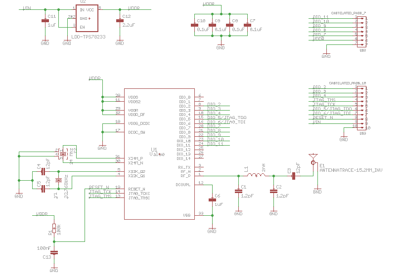
- i tried to use the same components they use (crystals, pasives, ...), and i think i use the same except for the inductor in the rf filter. TI uses LQG15HS2N0S02D (MuRata Inductor, Multilayer, Air Core, 2 nH, 0.3 A, 0.1 ohm, 0402) and i used L-07W2N0CV4T (JOHANSON TECHNOLOGY    high frecuency inductor, Serie L-07W, 2 nH, ± 0.2nH, 0402, 6 GHz, 0.07 oh).

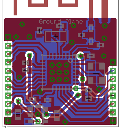
- Maybe a problem with the traces and the ground plane (picture below). There are ground plane in both top and bottom layers.

Schematic:
This is a picture of my PCB design:


  • Hello Juan,

    We will have our HW team take a look, but in the meantime, please review the "CC26xx HW Troubleshooting" article on the BLE wiki and confirm you have completed the check items.

    Also, please see the CC2640 sticky FAQ troubleshooting section "Q: Why am seeing poor RF performance and range issues on my custom CC2640 board when everything works fine on the TI Reference HW?" to confirm you have the proper SW settings in your project.

    Best wishes
  • Hi,

    Have you configured your SW correctly (5x5 with single ended front-end config and internal bias)? have you disabled the DCDC in SW? 

    Do you have a GND layer on the top layer like in our ref designs (looks like it since you have some vias)?

    How is DCDC_SW and VDDS_DCDC connected to GND?

    You need to improve the grounding so that all RF comp, decouplings and crystal comp hace separate GND vias. 

    Is the second layer a GND layer? The VDDS/VRRD routing in this layer should be moved so that it does not split the GND between the decoupling caps gnd and chip gnd. It should also be moved so that it is going around the 24 MHz crystal, not underneath like it is now. 

    It is true that the stack-up and comp type will affect the performance, but not this much. you have no tuning for the antenna so I assume you loose some performance there, please check out AN058. 

    Have you tested external power (no LDO) or adding a bead after the LDO?

  • Hi,

    I disabled in software the DCDC but i didn't know i have to configure "5x5 with single ended front-end config and internal bias" in software. I will do it.

    DCDC_SW and VDDS_DCDC are connected to top gorund plane. I have bottom and top ground plane. I put a image of the pcb with the ground planes:

    For the antenna i used ANO43. The cheapest and smallest footprint antenna i could find.

    i will redo the PCB to have separate GND vias for the decouplings and the crystal, and move the VDDS/VRRD routing to not split the GND plane and not behind the 24M crystal.

    i have not tested it with external power, but i'll try it and i show you the results.

    Thanks for your help,

    Regards.

  • well JXS answered it well. i have been going through kinda same problem, but the question regarding trace length is still unclear for small modules, the feed trace length has to be minimum so what can be the possible minimum feed trace length to get 50 ohm output impedance?
    also i used TX line to calculate the feed trace impedance and i found that length wasn't taking much part in creating 50 ohms it was width,height, copper pore thickness and ground plane distance from trace which was playing the part..length was changing electrical characteristic more but not the impedance
    and also here i can also see the balance port trace is also long isn't it gona effect the performance i think the rf components have to be nearest as possible to the balance port !!
  • I am note sure I understand your question. The external components in the RF match from the RF_N and RF_P pins must be placed close to the RF_P and RF_N pins. From the last comp in the RF filter/output from IPC you have a 50 ohm point and your trace between this point and the antenna should be a 50 ohm line. Before the antenna, you will need to place antenna tuning components (close to the antenna) to match the antenna to 50 ohm. the transmission line does not change impedance with length.