This thread has been locked.

If you have a related question, please click the "Ask a related question" button in the top right corner. The newly created question will be automatically linked to this question.

CC2640 Fatal error: Failed to do step: (Error -2134 @ 0x0) Unable to control device execution state

Other Parts Discussed in Thread: CC2640

Hi, I'm using smartrf06 board with our two different circuits both with CC2640 5CI package. We developed our firmware using the cc2650EM-7ID and now testing the same firmware with our custom boards. I'm also using ble stack v2.1.1 SimpleBLEBroadcaster with IAR for the application.

I can download and debug the firmware without any problem with one of the custom boards and everything works fine. When I do the exact same process with the second custom board which has the exact same RF configurations, LF clock, HF clock and circuit components, I can still download the firmware (both stack and the applicaiton). The problem is when I try to debug the same firmware with the second circuit I get the following error:

Fatal error: Failed to do step: (Error -2134 @ 0x0) Unable to control device execution state. Reset the device, and retry the operation. If error persists, confirm configuration, power-cycle the board, and/or try more reliable JTAG settings (e.g. lower TCLK). (Emulation package 6.0.83.1)

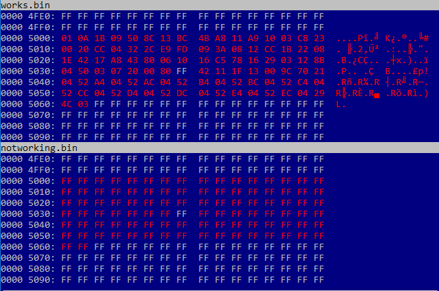
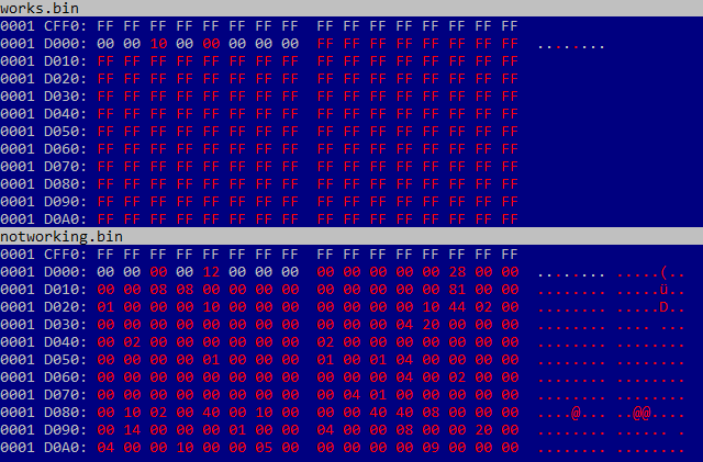
I followed the steps from iar_program_start function with the dis-assembly view and found out that the device comes in this state after executing the following line (0x23b6) which is inside the function "HapiTrimDeviceShutdown":

0x23b2: 0xf081 0x0101 EOR.W R1, R1, #1
0x23b6: 0x6081 STR R1, [R0, #0x8]
0x23b8: 0xb914 CBNZ R4, 0x23c0

where R1 = 0x00000001 and R0 = 0x43200000 at that moment.

I do the same steps with the other circuit design, I come to the same line with the exact register values and the code works without giving the same error.

Looking at this, one thinks it must be a board problem but both designs are exactly the same except some IO pins and we don't even mount those components on to the board. We tried everything such as changing the oscillators, using internal oscillator, changing the CC2640 on the circuit to be sure that it's not a defected one but nothing worked so far.

Can anyone help me with what could be the reason for this or what this line of code specifically does so that I can understand what could be the problem?

Thanks in advance.

  • Can you generate hex image and program into 2 devices. Read out the flash content by flash programmer 2 to compare see if there is something with JTAG on the second board?
  • Hi Christin,

    I did as you proposed and read all flash image to a binary file for both circuits. I then compared them with a binary compare tool and there were different parts. I added the different parts of the binary files below.

    Here the working circuit is "works" and the problematic circuit is "notworking". The addresses between the second snippet and the third one are almost all zeros, so the rest is also different from each other.

    Later I tried to flash the working image to the not working circuit with erase, program, verify steps with flash programmer. After all was successful and the reset of target was successful. But I still couldn't see BLE advertisement with packet sniffer so it was not working. I tried a reboot by powering off the smartrf06 board and powering it on again. After this attempt the module was bricked and it was not possible to see cc2640 with smart rf studio or flash programmer or sensor controller. I tried a forced massed erase with flash programmer but it was not possible either. We have bricked 4 cc2640 chips like this trying to understand what is the problem. I really don't want to brick another one.

    Now we changed the cc2640 on the circuit and I can see cc2640 again. I did the following steps with the new CC2640:

    1- I did a flash read with flash programmer which was successful where almost all the values are 0xFF except some at the end of flash which are 0xC5.

    2- I tried connecting to the device with Sensor Controller Studio but it gave the following error: "System CPU startup code failed. This may be due to incorrect target chip selection (name or revision)."

    3- I connected to the device with smart RF studio to see if there is a problem with the RF part. I can send a random TX packet and I can see this packet with packet sniffer when I use the working circuit. I copied all the configurations and executed a CMD_RADIO_SETUP command where I got an error with status "0xbad0". I couldn't find the reason for this status anywhere but looks like something is bad. :)

    After these steps I can still see automatically that the connected device is CC2640 with smart RF studio and flash programmer so the chip is not bricked yet. I'm confused about the reason for this problem. I could try downloading a basic code without the BLE stack like LED blink to see if there's a problem with that but I don't want to risk bricking another module. Can you help me about what could be the problem and how should I proceed? 

    Thanks,

  • It looks to me that JTAG might be the issue on the circuit, not CC26XX. Can you post your schematic and we can have out HW expert to take a look at it? Thanks!
  • Hi,
    I looked at the schematics and they look very similar. In both designs, I would change C2 to 22uF (as explained in the datasheet) since you are using a coincell battery. The load caps on the 32 kHz crystal looks small, but I guess you have the correct value. And also the 10 uH DCDC inductor is different than our ref designs, but I guess that you use the one from our ref design? What is R10 in your design that does not work, I would use a 0 ohm resistor.

    Have you tested with external power supply? How many boards have you tested, do you see the same error with all boards? Are the layout similar for the two boards? If not, can you send gerbers to Christin so that I can have a look at them? Have you done the steps in this wiki: processors.wiki.ti.com/.../CC26xx_HW_Troubleshooting
  • Hi Charlotte,

    Thank you for your help. I checked what you asked step by step and I'll try to answer them one by one.

    1 - We will change the C2 to 22uF when we have to use coincell battery but for now during development we are using the debugger as the source.

    2- We are aware of the 32 kHz crystal load caps but we are using the internal LF clock as the source for now so I'm guessing that is not the problem either.

    3- Actually we had 100 nH and apparently the problem was with the inductor. I'll explain in detail below.

    4- I tried using a 0 ohm resistor instead but the result is the same.

    5- We are already using the smart rf 06 board for debugging and testing so it is an external power supply.

    6- We have tested 2 boards with the working design and they all work perfectly. We then tested 5 boards with the not working design until now and 4 of them got bricked after we flashed the working image with flash programmer/IAR. So we see the same error with all of them.

    7- The layouts are almost similar except some parts.

    8- Actually we don't have the JTAG problem before flashing an image to the CC2640. I can connect to the device using both smart RF studio and flash programmer and it automatically detects CC2640. Flash programmer can perform a successful flash read with all values "0xFF". But the with the smart RF studio when I execute an CMD_RADIO_SETUP command it returns the status 0xbad0. But I can't connect to the second design with Sensor Controller Studio. To be sure I did all the steps from the link and they are all fine for both designs. (These were solved after 10uH inductor change)

    So we actually missed the 10 uH DCDC inductor in our designs but since they were the same in both designs (one working with 100nF and the other not) I didn't think it would be the problem. We didn't have a 10 uH in hand so I had to wait until we could try it so I checked others while waiting for it. When we changed the inductor in the circuit it was possible to connect to CC2640 with sensor controller and it was also possible to use smart RF studio where I executed a CMD_RADIO_SETUP and DONE_OK status returned. Since I thought the problem was solved I used flash programmer to write the working flash to the second design with new 10 uH inductor. I initiated the write but it returned error at the flash erase part. I then tried to read the flash but I had the following error:

    >Initiate access to target: XDS-06EB122129D7A.
    >Failed to read target memory.
    >Error while reading memory range. Address 0x40091090.
    >Debug interface is locked. Aborting action. Only forced mass erase is possible.
    >Reset target ...
    >Reset of target successfull.

    After this I did a forced mass erase with flash programmer which returned the following messages:

    >Initiate access to target: XDS-06EB122129D7A.
    >Failed to read target memory.
    >Error while reading memory range. Address 0x40091090.
    >Start flash erase ...
    >Erase finished successfully.
    >Reset target ...
    >Reset of target successfull.

    I tried another flash read but it failed again. I did another mass erase with the same returning messages. Then I disconnected everything from the computer and reconnected again. I opened sensor controller studio and tried to connect to the device but it gave the following error:

    "Register read operation failed"

    I opened flash programmer again but got the following error:

    "Debug interface is locked. Aborting action. Only forced mass erase is possible."

    So I did another mass erase but the result was the same. I then tried IAR to connect to the device but it gave the following error:

    "Error -241 A router subpath could not be accessed. A security error has probably occured."

    I also tried connecting with smart RF studio but had the following error:

    "Not able to open Device Control Panel. Check if Evaluation Board is already in use by another tool. Check jumpers on Evaluation Board. Device access failed: XBAL: Target connect failed."

    So I closed all the possible programs from Task Manager to be sure nothing is using the device. I then connected again with flash programmer but the result was the same. I searched this error in the forum but there were no successful answers. For example an answer is expected probably here as well:

    e2e.ti.com/.../1810324

    I believe we solved one problem with the inductor but caused another one I don't know how.

    In the end I believe it all comes to the question of: "Why does everything work perfectly with the first design since we are using the exact same components and not working properly with the second design?" That's why I want to ask the following questions:

    -What could be the reason that one design works with 100nH inductor and the other one does not?

    -How can I unbrick the CC2640 ?(if it's bricked because I can still detect it automatically with flash programmer)

    By the way I checked other answers of this problem in forum and also checked RST,TCK,TMS,GND pins are well connected as well as 1.68V and 1.27V is seen at the respective pins.

    Thanks
  • The DCDC inductor is very important if using the internal DCDC and you must use the one from our reference design. Using a different vendor for this comp may also cause issues, so I would use the same as we have in our reference designs. Do you have the DCDC on or off in your code (this can be set in SW)?I looked at the designs quickly, and noticed that for the non working design, in addition to the wrong inductor, the traces to the external DCDC cap and inductor are long which is not recommended and can cause noise. If the DCDC is on and you have the wrong inductor you can brick the device and also destroy it. Have you tested a new non-working board with the correct inductor in place to start with? Or with the DCDC off to start of with? 

  • We were using the same components from your reference design except that inductor (100nH) and it was working only with the smaller design but not with the bigger design. Now we changed the inductor to 10 uH with a new device, tested the new board step by step since Tuesday and it works well until now. I always had the DCDC on in the code and it works fine now with the 10uH inductor as well. Even though the design works like this we will also keep in mind the long traces and try to shorten them on further development. Thank you very much for your help on the topic.

    My only question is that if it would be possible to unbrick (if it's bricked) the CC2640 on the old board which I get the following error as I stated in my last post when I try to connect with flash programmer:

    >Initiate access to target: XDS-06EB122129D7A.
    >Failed to read target memory.
    >Error while reading memory range. Address 0x40091090.
    >Debug interface is locked. Aborting action. Only forced mass erase is possible.
    >Reset target ...
    >Reset of target successfull.

    After this I did a forced mass erase with flash programmer which returned the following messages:

    >Initiate access to target: XDS-06EB122129D7A.
    >Failed to read target memory.
    >Error while reading memory range. Address 0x40091090.
    >Start flash erase ...
    >Erase finished successfully.
    >Reset target ...
    >Reset of target successfull.

    Now flash programmer can detect automatically that it's a CC2640 and I can read the normal VDDS_DCDC, DCOUPL, VDDR and VDDR_RF voltage values so I'm guessing it's a different problem. What could be the solution?

    Thanks,

    Ogulcan
  • Can you try to just read back the flash content? see if it's possible to access the flash?
  • I tried it with flash programmer but the error is the same:

    >Initiate access to target: XDS-06EB122129D7A.

    >Failed to read target memory.

    >Error while reading memory range. Address 0x40091090.

    >Debug interface is locked. Aborting action. Only forced mass erase is possible.

    >Reset target ...

    >Reset of target successfull.

  • If the debug interface is locked, then there is no way to unbrick the device.