This thread has been locked.

If you have a related question, please click the "Ask a related question" button in the top right corner. The newly created question will be automatically linked to this question.

CC2650 RF front end

Other Parts Discussed in Thread: CC2650

Hi,

Please look at the below image of the evaluation schematic from CC2650 launch pad and sensor tag

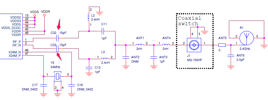
Sensor tag RF front end :

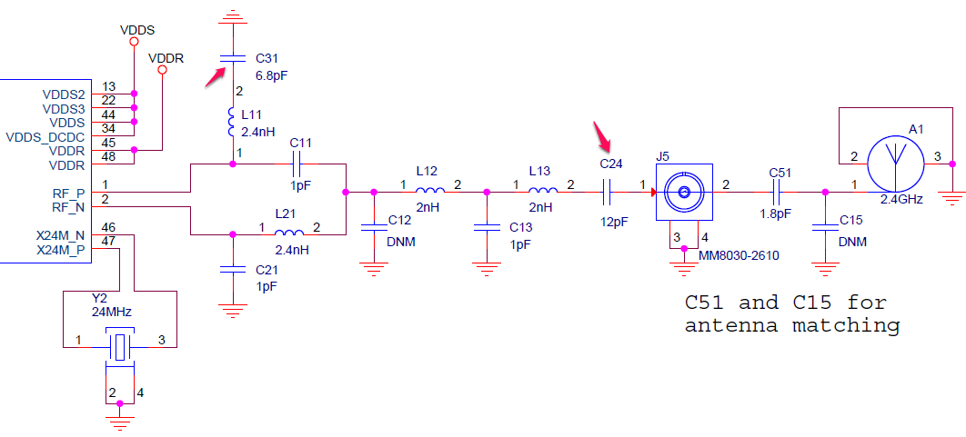
Launch pad Rf front end :

1. On the Sensor tag evaluation kit schematic no DC blocking capacitor is used. Can I please know the reason for using C32 and C33 (15pF) capacitor on pin 1 and 2 of CC2650.

2. On the launch pad evaluation kit schematic, capacitor C24 (12pF) is used as a DC blocking capacitor. Can I also please know the reason for using C31 (6.8pF) next to L11 (2.4nH)

I would like to know which design should I need to follow. 

Thanks.

Regards,

Vikash. 

  • On the sensortag design, the C32 and C33 are the DC blocks and are moved to the RF pins. On the reference design for the EM, they are placed at the end C24 and in the balun C31. Both will work when using internal bias. If using external bias, the DC blocks cannot be placed like in the sensortag design and the reference design for the EM must be followed.
  • Hi, in order to comply with ETSI requirements which RF front design design should be used? We are creating a temperature & humidity sensor based on the TI CC2650 sensortag reference design. Is the RF front end design for the sensortag sufficient for this?

    Thank you

  • Hi Sarwar,

    All the TI reference designs have been measured to be compliant with FCC and ETSI requirements. Of course, the performance will depend on your specific board design, so some RF tuning might be necessary to both achieve good performance and also be compliant to regulatory rules.

    Cheers,
    Fredrik