This thread has been locked.

If you have a related question, please click the "Ask a related question" button in the top right corner. The newly created question will be automatically linked to this question.

CC2650 smallest timer interrupt resolution

Other Parts Discussed in Thread: CC2650

I am working on CC2650 sensortag to generate precise timer interrupt. I need timer interrupt to be triggered every 500 ns.

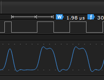
Referring to CC2650 is running at 48 MHz, ideally it should be possible to generate a timer interrupt in nano seconds range. However, in my testing the smallest timer intterupt period that i can achieve is around 1.5 us

(i use oscilloscope to monitor BDP2 = IOID_23)

The following is my code:

void Timer0Isr()
{
TimerIntClear(GPT2_BASE, TIMER_TIMA_TIMEOUT);
PIN_setOutputValue(ledPinHandle2, BDP2, iTog); //BDP2 = IOID_23
iTog = (iTog ? 0 : 1);
}

void TimerSetup()
{
PRCMPowerDomainOn(PRCM_DOMAIN_PERIPH);
PRCMLoadSet();
PRCMPeripheralRunEnable(PRCM_PERIPH_TIMER2); // Enables a peripheral Timer
PRCMLoadSet();

TimerDisable(GPT2_BASE, TIMER_BOTH);//TimerDisable(GPT0_BASE, TIMER_BOTH); // Timer disable
TimerConfigure( GPT2_BASE,TIMER_CFG_SPLIT_PAIR | TIMER_CFG_A_PERIODIC_UP ); // TIMER_CFG_A_PERIODIC );
TimerLoadSet(GPT2_BASE, TIMER_A, 2); // 100 = ~ 2us, 75 = ~1.5us, try to goes below has no effect
TimerIntRegister(GPT2_BASE, TIMER_A, Timer0Isr); // Link timer interrupt with Timer0Isr
TimerIntEnable(GPT2_BASE,TIMER_TIMA_TIMEOUT);// TIMER_TIMA_TIMEOUT); // Enables individual timer interrupt sources.
TimerEnable(GPT2_BASE, TIMER_A); // Timer Enable}
IntMasterEnable();
}

Is the delay due to call back function overhead? How can i achieve timer intterrupt below 1 us range?

NB: i have taken out POWER_SAVING setting this project

Thank you in advance. Any assistance from the forum / TI support will be very much appreciated.

  • In my further testing i found out that the limitation could be caused by the I/O toggle process on CC2650
    I created another testing project which basically run into a while loop and keep toggle 1 I/O

    while(1)
    {
    PIN_setOutputValue(ledPinHandle2, BDP2, iTog); //BDP2 = IOID_23
    iTog = (iTog ? 0 : 1);
    }

    The result whic i get by monitoring IOID_23 on my oscilloscope is the time it takes for the I/O pin from High to Low / Low to High is around 1 us.

    TI support team please help to look into this
  • Can you elaborate what you want to do every 500ns? Just toggle IOs? If that's the case, will you consider using PWM driver to generate IO toggling with 500ns period?

    Please noted that the load capacitance introduced by probing will affect the IO transition rate.
  • Hi Chirstin,

    i need to generate a sequence of pulse to transmit code 0 and code 1 following the following timing diagram by toggling 1 I/O on CC2650

    tolerance for each pulse is only around +/- 150 ns. Hence, i need a fast I/O toggling using precise timer intterupt which has smallest resolution of 0.5 us (500 ns)

    If i use PWM driver as you suggested, will it help? because it seems like the limitation on how fast we can toggle an I/O from high to low / low to high on CC2650

    Regards,

    Handy

  • Hi,

    In order to change duty cycle on the fly, you can't use PWM driver unfortunately.

    I have done some low level register access to implement a one time 0 code+ one time 1 code.

    What I did was: 

    1. Set up timer0A as PWM and timer0B as one shot match mode with the same period

        
        //configure timer0 A as PWM, timer0 B as compare mode for match event
        TimerConfigure(GPT0_BASE, TIMER_CFG_SPLIT_PAIR | TIMER_CFG_A_PWM | TIMER_CFG_A_PERIODIC_UP | TIMER_CFG_B_ONE_SHOT);
        
        //timer0A 2.5u period, 80% duty cycle, starts right away but idle as low
        TimerMatchSet(GPT0_BASE, TIMER_A, 0x5F);
        
        // 2.5us period = 120-1 ticks. Timer starts to count from 119 and wraps around when counter reaches 0
        TimerLoadSet(GPT0_BASE, TIMER_A, 0x77);
       
        // Event0 is mapped to timer0A
        IOCPortConfigureSet(Board_LED1, IOC_PORT_MCU_PORT_EVENT0, IOC_NO_IOPULL | IOC_CURRENT_8MA |IOC_SLEW_DISABLE);
    
        //Set the starting value for timer B
        TimerLoadSet(GPT0_BASE, TIMER_B, 130);
        //Set the match value for timer B
        TimerMatchSet(GPT0_BASE, TIMER_B, 11);
        
        // enable DMA trigger when timer B match
        HWREG(GPT0_BASE + GPT_O_DMAEV) = GPT_DMAEV_TBMDMAEN;

    2. set up DMA to transfer the new dutycycle value when timer0B matches

      
        // Enable uDMA power domain
        PRCMLoadSet();
        PRCMPeripheralRunEnable(PRCM_PERIPH_UDMA);
        PRCMLoadSet();
        
        //
        // Set the base for the channel control table.
        //
        uDMAControlBaseSet(UDMA0_BASE, (void *) UDMACC26XX_CONFIG_BASE);
        uDMAEnable(UDMA0_BASE);
        
        //
        // Now set up the characteristics of the transfer.  It will
        // be 8 bit data size, with no increment in source and destination.
        // 1 byte copy is performed
        //
        uDMAChannelControlSet(UDMA0_BASE, UDMA_CHAN_TIMER0_B | UDMA_PRI_SELECT, //ch #9
                              UDMA_SIZE_8 | UDMA_SRC_INC_NONE |
                                UDMA_DST_INC_NONE |
                                  UDMA_ARB_8);
        
        uDMAChannelTransferSet(UDMA0_BASE, UDMA_CHAN_TIMER0_B | UDMA_PRI_SELECT, //ch #9
                               UDMA_MODE_BASIC, //single transfer
                               &registerValue[count],//source address
                               (void *)(GPT0_BASE + GPT_O_TAMATCHR), //destination address
                               1);
        
        uDMAChannelEnable(UDMA0_BASE, UDMA_CHAN_TIMER0_B);
    static uint8_t registerValue[10] = {0x3B, 0x17, 0x3B, 0x3B, 0x17, 0x3B, 0x17, 0x3B, 0x17, 0x3B};

    3. start timer0A and timer0B together

    The code above is just to help you getting started. You will still have to re-arm the DMA and probably more

  • 1 us latency is caused by PIN_setOutputValue(), when i change the function call using:

    PIN_setOutputValue(ledPinHandle2, BDP2, 1);

    PIN_setOutputValue(ledPinHandle2, BDP2, 0);

    --> toggle from high to low is about 1 us

    GPIOPinWrite(GPIO_PIN_23,1);

    GPIOPinWrite(GPIO_PIN_23,0);

    --> toggle from high to low is about 40 ns

    However, it is also quite a difficult to generate precise code 0 and code 1 using timer intterrupt, the more data processing we need to do on the ISR callback the more delay we will get. In my testing, if we handle GPIO toggle using ISR callback,  the callback it self has introduce about 470 ns delay to the I/O toggling

    My ISR callback and timer setup is as follow:

    void Timer0Isr()

    {

    TimerIntClear(GPT2_BASE, TIMER_TIMA_TIMEOUT);

    GPIOPinToggle(GPIO_PIN_23);

    }

    void TimerSetup()

    {

    PRCMPeripheralRunEnable(PRCM_PERIPH_TIMER2); // Enables a peripheral Timer

    PRCMLoadSet();

    TimerDisable(GPT2_BASE, TIMER_BOTH);//TimerDisable(GPT0_BASE, TIMER_BOTH); // Timer disable

    TimerConfigure( GPT2_BASE,TIMER_CFG_A_PERIODIC );

    TimerLoadSet(GPT2_BASE, TIMER_A, 1);

    TimerIntRegister(GPT2_BASE, TIMER_A, Timer0Isr); // Link timer interrupt with Timer0Isr

    TimerIntEnable(GPT2_BASE,TIMER_TIMA_TIMEOUT);

    TimerEnable(GPT2_BASE, TIMER_A); // Timer Enable}

    IntMasterEnable();

    }

    If we keep adding data processing logic to control the sequence and control the waveform of code 1 and code 0 inside Timer0Isr, the delay is getting bigger and bigger and make it very difficult to has precise sequence of code 0 and code 1.

    Please let me know if there is a better way to achieve this. I want to use CC2650 to transmit 24 bit sequence of code 0 and 1 following the timing diagram in my previous post.

    Regards,

    Handy

  • Hi,

    You can't achieve what you want by using HW interrupt. Have you checked out what I posted above? 

  • Dear Christin,

    Thank you for your hints. I managed to reproduce the code 1 and code 0 using timer A PWM and adjust the duty cycle accordingly.
    Using timer B to change the GPT_O_TAMATCHR is also very interesting concept to minimize the delay.
    However, in order to re-arm the uDMAChannelTransferSet() with different value when Timer B value match event happen, we need to implement something like call back function (ISR) for Timer B.
    Call back function will introduce some delay. My concern is if timer A and timer B out of sync, the pattern of code 1 and code 0 sequence generated will be wrong as well.

    Can you suggest a more efficient way to re-arm the Timer A GPT_O_TAMATCHR value using uDMAChannelTransferSet() in a highly precise timing?

    Regards,
    handy