


Part Number: CC2650
Hi everyone!
We are designing a PCB equipped with CC2650F128RSMR SimpleLink MCU. We have an accelerometer and it will communicate through SPI to the MCU, which will use the Embedded Bluetooth to a smartphone.
We are experiencing some issues for the design of the antenna interface. We found online support and the schematic of the Sensor Tag and the BoostKit for a PCB traced antenna, but we should use a chip antenna by Johanson Technlogy: 2450AT07A0100, a chip antenna requiring ground clearance.
We are sorry if some questions may seem too obvious, but it's the first time we come across this kind of challenges. Any help and link to available material will be much appreciated! :)
Please refer to the schematics of the SimpleLink™ CC2650 Wireless MCU LaunchPad™ Kit, here a detail about the RF section:
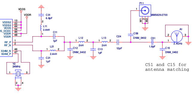
1. Can we exploit the scheme adopted for the boostkit of the CC2650, as indicated in the schematic for what concerns the differential mode circuit and the filter right ahead even if we are changing the antenna?
2. The removal of the unused coaxial switch has some impacts in the circuitry to be inserted?
The antenna manufacturer (see link above) suggests a pi-matching network (shunt-series-shunt), plus an ad-hoc sized width line (to guarantee 50 ohms matched impedance)
3. Is the pi-network needed after all this circuitry (if so how components should be placed and where) or the filter stages in the schematic provide already a good interface?
4. Where the trace width should be adjusted to guarantee 50 ohms? (after c12? c24 or just at the end, before the antenna?) and should the components be placed close to the MCU or closer to the Antenna to guarantee best noise immunity and performance?
Thanks in advance for your help! :)
Marco De Clemente
Embedded Systems Electr. Engineering - Turin - Italy
