Other Parts Discussed in Thread: CC2640R2F, CC2640
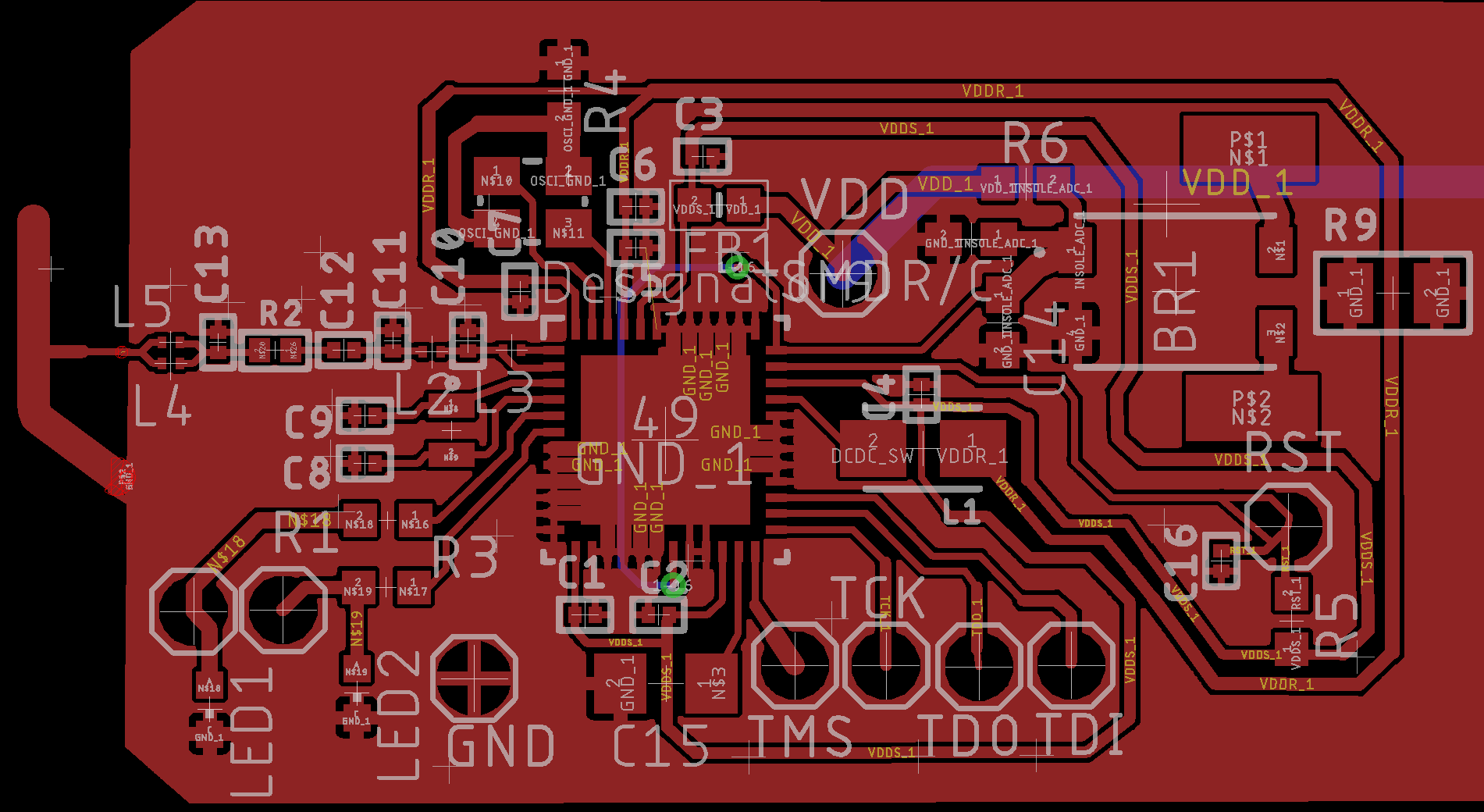
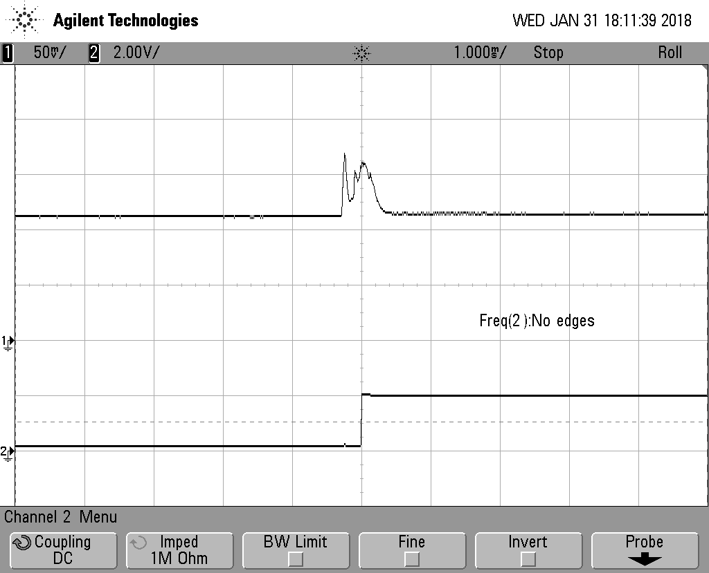
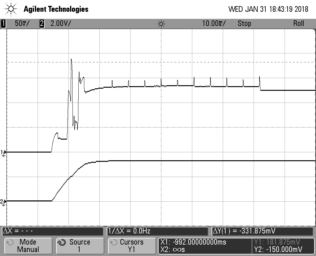
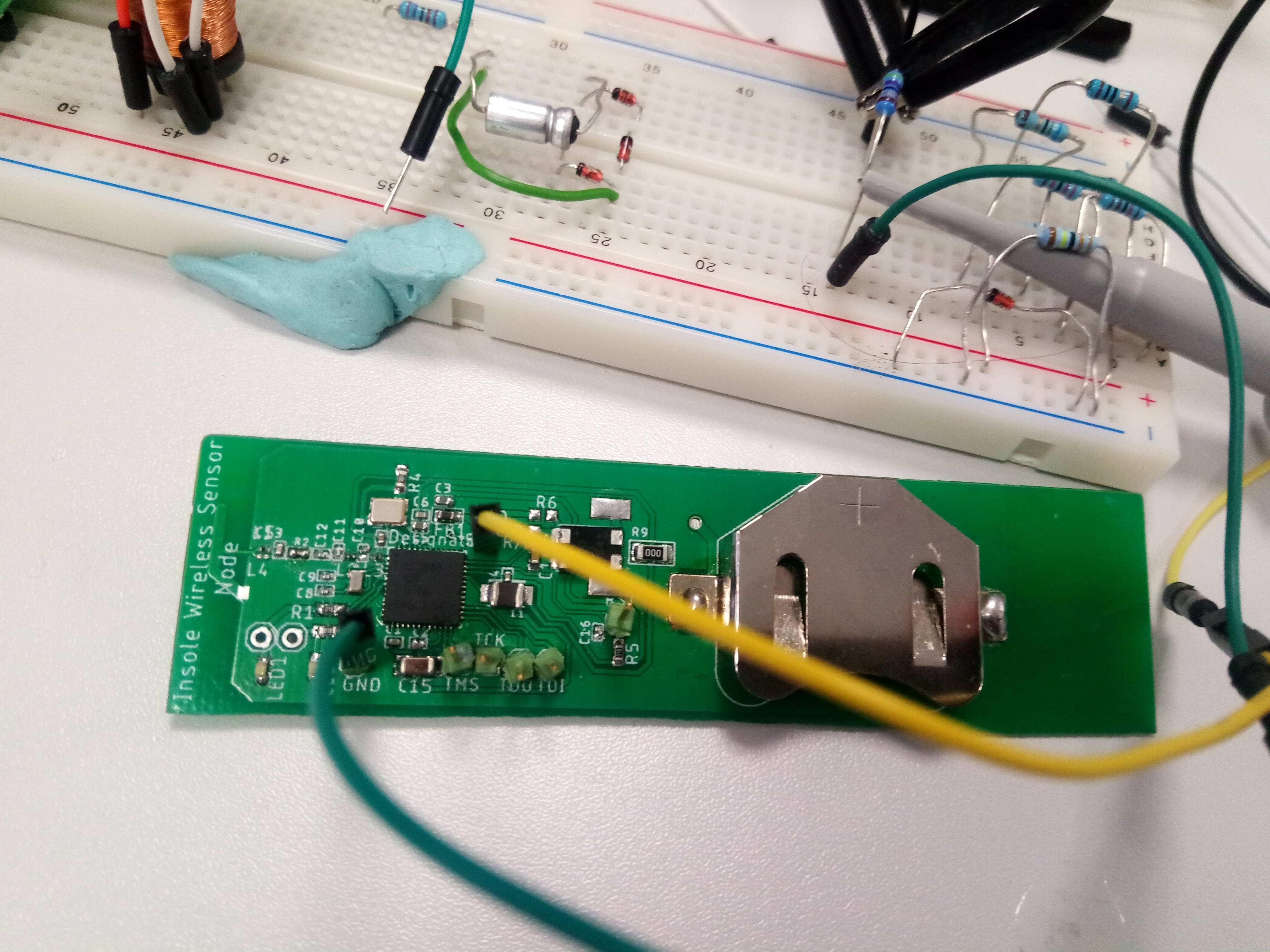
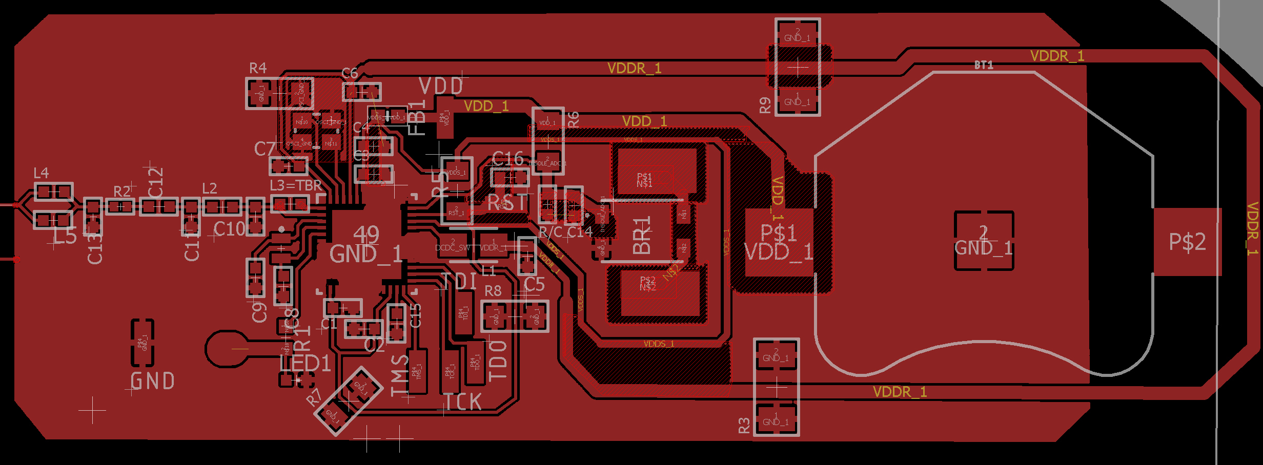
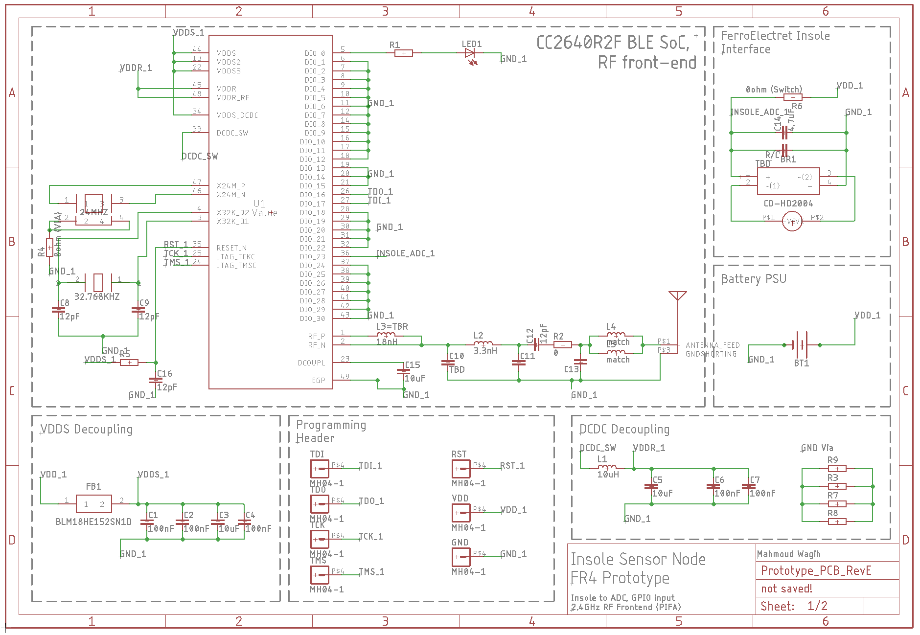
I have designed a custom board, my board design is intended for a single layer PCB so I have routed all the unused pins to the exposed ground pad, as shown in the attached layout picture. I have measured the current consumption of the board while running the pinstandby example, a current consumption of >16mA is measured while the device is supposed to be in sleep mode. Do I need to have to initialize the pins in a certain way to prevent the current from leaking through the grounded GPIO pins?
I am currently trying to design a new antenna for the flexible circuit I am designing, the antenna in the layout is tested using a VNA and has a similar gain to the reference design, I couldn't however receive the bluetooth advertisement on a smartphone app? I couldn't confirm that the device is transmitting using an oscilloscope to measure the current drawn, as it is constantly >30mA when running the simple broadcaster example.
Thanks
Mahmoud