This thread has been locked.

If you have a related question, please click the "Ask a related question" button in the top right corner. The newly created question will be automatically linked to this question.

CC2640R2F: The chip is locked and can not be recovered.

Part Number: CC2640R2F
Other Parts Discussed in Thread: CC2640

Hi All

Target board: CC2640R2 launchpad

The damage chip can not do any function on Flashprogrammer2 and shows it is locked.

Follow the tips to force mass erase the chip. Flashprogrammer2 shows success, but CC2640R2 can not handle any debug commands(Erase, Program, Read).

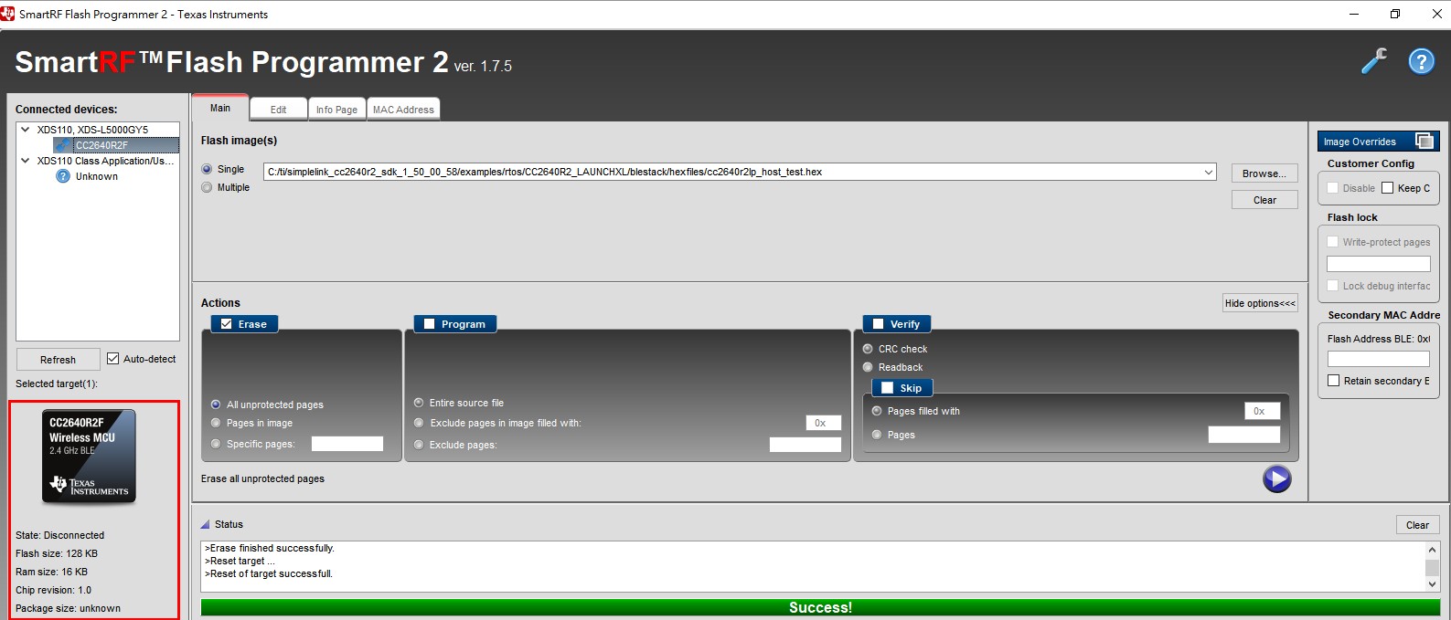
After the mass erase is done, the strange situation is that flashprogrammer2 shows that the RAM size is 16KB(normal is 20KB), and package size shows unknow(normal is 7x7).

Before the chip is locked, it was using SPI bootloader to update the FW. Somehow, the cc2640 shows locked on flashprogrammer2 when we want to Erase the chip.

This problem happened twice (normally, there is no such problem), so we have 2 CC2640R2 has been damaged and can not be recovered. Note that the bootloader update includes the CCFG area. 

BR,

Jack

  • Hi Jack,

    It is possible to go into this state by locking access to the debug system in CCFG. What is the content of the CCFG update? Are you using the ROM bootloader or something else?

    Cheers,
    Fredrik
  • Hi Fredrik,

    Yes, using ROM Bootloader for update FW.

    The most content of CCFG is base on default of  BLE example. But Changes the setting of  bootloader.

    Provide the CCFG file and the SPI analyze data. Software of SPI analyze :

    https://e2e.ti.com/cfs-file/__key/communityserver-discussions-components-files/538/cc2640_5F00_FWU_5F00_SPI.7z

    /******************************************************************************
    
     @file       ccfg_app_ble.c
    
     @brief Customer Configuration CC26xx PG2 device family.
    
     Group: CMCU, SCS
     Target Device: CC2640R2
    
     ******************************************************************************
     
     Copyright (c) 2014-2017, Texas Instruments Incorporated
     All rights reserved.
    
     Redistribution and use in source and binary forms, with or without
     modification, are permitted provided that the following conditions
     are met:
    
     *  Redistributions of source code must retain the above copyright
        notice, this list of conditions and the following disclaimer.
    
     *  Redistributions in binary form must reproduce the above copyright
        notice, this list of conditions and the following disclaimer in the
        documentation and/or other materials provided with the distribution.
    
     *  Neither the name of Texas Instruments Incorporated nor the names of
        its contributors may be used to endorse or promote products derived
        from this software without specific prior written permission.
    
     THIS SOFTWARE IS PROVIDED BY THE COPYRIGHT HOLDERS AND CONTRIBUTORS "AS IS"
     AND ANY EXPRESS OR IMPLIED WARRANTIES, INCLUDING, BUT NOT LIMITED TO,
     THE IMPLIED WARRANTIES OF MERCHANTABILITY AND FITNESS FOR A PARTICULAR
     PURPOSE ARE DISCLAIMED. IN NO EVENT SHALL THE COPYRIGHT OWNER OR
     CONTRIBUTORS BE LIABLE FOR ANY DIRECT, INDIRECT, INCIDENTAL, SPECIAL,
     EXEMPLARY, OR CONSEQUENTIAL DAMAGES (INCLUDING, BUT NOT LIMITED TO,
     PROCUREMENT OF SUBSTITUTE GOODS OR SERVICES; LOSS OF USE, DATA, OR PROFITS;
     OR BUSINESS INTERRUPTION) HOWEVER CAUSED AND ON ANY THEORY OF LIABILITY,
     WHETHER IN CONTRACT, STRICT LIABILITY, OR TORT (INCLUDING NEGLIGENCE OR
     OTHERWISE) ARISING IN ANY WAY OUT OF THE USE OF THIS SOFTWARE,
     EVEN IF ADVISED OF THE POSSIBILITY OF SUCH DAMAGE.
    
     ******************************************************************************
     Release Name: simplelink_cc2640r2_sdk_ble_example_pack_01_50_00_62
     Release Date: 2017-11-01 10:38:41
     *****************************************************************************/
    
    //
    //       ===> READ THIS BEFORE MODIFYING THIS FILE
    //
    //
    //       ===> READ THIS BEFORE MODIFYING THIS FILE
    //
    //
    //       ===> READ THIS BEFORE MODIFYING THIS FILE
    //
    
    // The customer configuration area (ccfg section) is located at the end of the
    // flash and reflect the hw configuration of the device. it is very important
    // that it remains align with the version of driverlib you are using.
    // all BLE project except sensor tag use the same configuration.
    // Keeping the "#include <startup_files/ccfg.c>" guarantee that your project using
    // driverlib and the ccfg area will be align.
    
    // you can modify it if you want, the recommend way will be to remove the
    // bellow include, copy the content of the <startup_files/ccfg.c> file in this
    // file and rebuild.
    
    // ==> KEEP IN MIND that if you do so, be sure that any further update of the
    // driverlib must be align with your modified version of ccfg area.
    //#include <startup_files/ccfg.c>
    
    
    #ifndef __CCFC_C__
    #define __CCFC_C__
    
    #include <stdint.h>
    #include "inc/hw_types.h"
    #include "inc/hw_ccfg.h"
    #include "inc/hw_ccfg_simple_struct.h"
    
    //*****************************************************************************
    //
    // Introduction
    //
    // This file contains fields used by Boot ROM, startup code, and SW radio 
    // stacks to configure chip behavior.
    //
    // Fields are documented in more details in hw_ccfg.h and CCFG.html in 
    // DriverLib documentation (doc_overview.html -> CPU Domain Memory Map -> CCFG).
    //
    // PLEASE NOTE:
    // It is not recommended to do modifications inside the ccfg.c file.
    // This file is part of the CoreSDK release and future releases may have
    // important modifications and new fields added without notice.
    // The recommended method to modify the CCFG settings is to have your
    // own <customer_ccfg>.c file that defines the specific CCFG values to be
    // overridden and finally including ccfg.c from the <customer_ccfg>.c file.
    //
    // Example:
    // #define SET_CCFG_BL_CONFIG_BOOTLOADER_ENABLE  0xC5 // Enable ROM boot loader
    // #define SET_CCFG_MODE_CONF_SCLK_LF_OPTION     0x3  // LF RCOSC
    // //---- Use default values for all others ----
    // #include "<project-path>/source/ti/devices/<device>/startup_files/ccfg.c"
    // 
    //*****************************************************************************
    
    //*****************************************************************************
    //
    // Set the values of the individual bit fields.
    //
    //*****************************************************************************
    
    //#####################################
    // Alternative DC/DC settings
    //#####################################
    
    #ifndef SET_CCFG_SIZE_AND_DIS_FLAGS_DIS_ALT_DCDC_SETTING
    #define SET_CCFG_SIZE_AND_DIS_FLAGS_DIS_ALT_DCDC_SETTING    0x0    // Alternative DC/DC setting enabled
    // #define SET_CCFG_SIZE_AND_DIS_FLAGS_DIS_ALT_DCDC_SETTING 0x1    // Alternative DC/DC setting disabled
    #endif
    
    #ifndef SET_CCFG_MODE_CONF_1_ALT_DCDC_VMIN
    #define SET_CCFG_MODE_CONF_1_ALT_DCDC_VMIN              0x8        // 2.25V
    #endif
    
    #ifndef SET_CCFG_MODE_CONF_1_ALT_DCDC_DITHER_EN
    #define SET_CCFG_MODE_CONF_1_ALT_DCDC_DITHER_EN         0x0        // Disable
    // #define SET_CCFG_MODE_CONF_1_ALT_DCDC_DITHER_EN      0x1        // Enable
    #endif
    
    #ifndef SET_CCFG_MODE_CONF_1_ALT_DCDC_IPEAK
    #define SET_CCFG_MODE_CONF_1_ALT_DCDC_IPEAK             0x2        // 39mA
    #endif
    
    //#####################################
    // XOSC override settings
    //#####################################
    
    #ifndef SET_CCFG_SIZE_AND_DIS_FLAGS_DIS_XOSC_OVR
    // #define SET_CCFG_SIZE_AND_DIS_FLAGS_DIS_XOSC_OVR     0x0        // Enable override
    #define SET_CCFG_SIZE_AND_DIS_FLAGS_DIS_XOSC_OVR        0x1        // Disable override
    #endif
    
    #ifndef SET_CCFG_MODE_CONF_1_DELTA_IBIAS_INIT
    #define SET_CCFG_MODE_CONF_1_DELTA_IBIAS_INIT           0x0        // Delta = 0
    #endif
    
    #ifndef SET_CCFG_MODE_CONF_1_DELTA_IBIAS_OFFSET
    #define SET_CCFG_MODE_CONF_1_DELTA_IBIAS_OFFSET         0x0        // Delta = 0
    #endif
    
    #ifndef SET_CCFG_MODE_CONF_1_XOSC_MAX_START
    #define SET_CCFG_MODE_CONF_1_XOSC_MAX_START             0x10       // 1600us
    #endif
    
    //#####################################
    // Power settings
    //#####################################
    
    #ifndef SET_CCFG_MODE_CONF_VDDR_TRIM_SLEEP_DELTA
    #define SET_CCFG_MODE_CONF_VDDR_TRIM_SLEEP_DELTA        0xF        // Signed delta value +1 to apply to the VDDR_TRIM_SLEEP target (0xF=-1=default=no compensation)
    #endif
    
    #ifndef SET_CCFG_MODE_CONF_DCDC_RECHARGE
    #define SET_CCFG_MODE_CONF_DCDC_RECHARGE                0x0        // Use the DC/DC during recharge in powerdown
    // #define SET_CCFG_MODE_CONF_DCDC_RECHARGE             0x1        // Do not use the DC/DC during recharge in powerdown
    #endif
    
    #ifndef SET_CCFG_MODE_CONF_DCDC_ACTIVE
    #define SET_CCFG_MODE_CONF_DCDC_ACTIVE                  0x0        // Use the DC/DC during active mode
    // #define SET_CCFG_MODE_CONF_DCDC_ACTIVE               0x1        // Do not use the DC/DC during active mode
    #endif
    
    #ifndef SET_CCFG_MODE_CONF_VDDS_BOD_LEVEL
    // #define SET_CCFG_MODE_CONF_VDDS_BOD_LEVEL            0x0        // VDDS BOD level is 2.0V
    #define SET_CCFG_MODE_CONF_VDDS_BOD_LEVEL               0x1        // VDDS BOD level is 1.8V (or 1.65V for external regulator mode)
    #endif
    
    #ifndef SET_CCFG_MODE_CONF_VDDR_CAP
    #define SET_CCFG_MODE_CONF_VDDR_CAP                     0x3A       // Unsigned 8-bit integer representing the min. decoupling capacitance on VDDR in units of 100nF
    #endif
    
    #ifndef SET_CCFG_MODE_CONF_VDDR_TRIM_SLEEP_TC
    #define SET_CCFG_MODE_CONF_VDDR_TRIM_SLEEP_TC           0x1        // Temperature compensation on VDDR sleep trim disabled (default)
    // #define SET_CCFG_MODE_CONF_VDDR_TRIM_SLEEP_TC        0x0        // Temperature compensation on VDDR sleep trim enabled
    #endif
    
    //#####################################
    // Clock settings
    //#####################################
    
    #ifndef SET_CCFG_MODE_CONF_SCLK_LF_OPTION
    // #define SET_CCFG_MODE_CONF_SCLK_LF_OPTION            0x0        // LF clock derived from High Frequency XOSC
    // #define SET_CCFG_MODE_CONF_SCLK_LF_OPTION            0x1        // External LF clock
    #define SET_CCFG_MODE_CONF_SCLK_LF_OPTION               0x2        // LF XOSC
    // #define SET_CCFG_MODE_CONF_SCLK_LF_OPTION            0x3        // LF RCOSC
    #endif
    
    #ifndef SET_CCFG_MODE_CONF_XOSC_CAP_MOD
    // #define SET_CCFG_MODE_CONF_XOSC_CAP_MOD              0x0        // Apply cap-array delta
    #define SET_CCFG_MODE_CONF_XOSC_CAP_MOD                 0x1        // Don't apply cap-array delta 
    #endif
    
    #ifndef SET_CCFG_MODE_CONF_XOSC_CAPARRAY_DELTA
    #define SET_CCFG_MODE_CONF_XOSC_CAPARRAY_DELTA          0xFF       // Signed 8-bit value, directly modifying trimmed XOSC cap-array value
    #endif
    
    #ifndef SET_CCFG_EXT_LF_CLK_DIO
    #define SET_CCFG_EXT_LF_CLK_DIO                         0x01       // DIO number if using external LF clock
    #endif
    
    #ifndef SET_CCFG_EXT_LF_CLK_RTC_INCREMENT
    #define SET_CCFG_EXT_LF_CLK_RTC_INCREMENT               0x800000   // RTC increment representing the external LF clock frequency
    #endif
    
    //#####################################
    // Special HF clock source setting
    //#####################################
    #ifndef SET_CCFG_MODE_CONF_XOSC_FREQ
    // #define SET_CCFG_MODE_CONF_XOSC_FREQ                 0x1        // Use HPOSC as HF source (if executing on a HPOSC chip, otherwise using default (=0x3))
    // #define SET_CCFG_MODE_CONF_XOSC_FREQ                 0x2        // HF source is a 48 MHz xtal
    #define SET_CCFG_MODE_CONF_XOSC_FREQ                    0x3        // HF source is a 24 MHz xtal (default)
    #endif
    
    //#####################################
    // Bootloader settings
    //#####################################
    
    #ifndef SET_CCFG_BL_CONFIG_BOOTLOADER_ENABLE
    //#define SET_CCFG_BL_CONFIG_BOOTLOADER_ENABLE            0x00       // Disable ROM boot loader
    #define SET_CCFG_BL_CONFIG_BOOTLOADER_ENABLE            0xC5       // Enable ROM boot loader
    #endif
    
    #ifndef SET_CCFG_BL_CONFIG_BL_LEVEL
    #define SET_CCFG_BL_CONFIG_BL_LEVEL                     0x0        // Active low to open boot loader backdoor
    //#define SET_CCFG_BL_CONFIG_BL_LEVEL                     0x1        // Active high to open boot loader backdoor
    #endif
    
    #ifndef SET_CCFG_BL_CONFIG_BL_PIN_NUMBER
    //#define SET_CCFG_BL_CONFIG_BL_PIN_NUMBER                0xFF       // DIO number for boot loader backdoor
    #define SET_CCFG_BL_CONFIG_BL_PIN_NUMBER                0x0D       // DIO number for boot loader backdoor
    #endif
    
    #ifndef SET_CCFG_BL_CONFIG_BL_ENABLE
    #define SET_CCFG_BL_CONFIG_BL_ENABLE                    0xC5       // Enabled boot loader backdoor
    //#define SET_CCFG_BL_CONFIG_BL_ENABLE                    0xFF       // Disabled boot loader backdoor
    #endif
    
    //#####################################
    // Debug access settings
    //#####################################
    
    #ifndef SET_CCFG_CCFG_TI_OPTIONS_TI_FA_ENABLE
    #define SET_CCFG_CCFG_TI_OPTIONS_TI_FA_ENABLE           0x00       // Disable unlocking of TI FA option.
    // #define SET_CCFG_CCFG_TI_OPTIONS_TI_FA_ENABLE        0xC5       // Enable unlocking of TI FA option with the unlock code
    #endif
    
    #ifndef SET_CCFG_CCFG_TAP_DAP_0_CPU_DAP_ENABLE
    // #define SET_CCFG_CCFG_TAP_DAP_0_CPU_DAP_ENABLE       0x00       // Access disabled
    #define SET_CCFG_CCFG_TAP_DAP_0_CPU_DAP_ENABLE          0xC5       // Access enabled if also enabled in FCFG
    #endif
    
    #ifndef SET_CCFG_CCFG_TAP_DAP_0_PRCM_TAP_ENABLE
    #define SET_CCFG_CCFG_TAP_DAP_0_PRCM_TAP_ENABLE         0x00       // Access disabled
    // #define SET_CCFG_CCFG_TAP_DAP_0_PRCM_TAP_ENABLE      0xC5       // Access enabled if also enabled in FCFG
    #endif
    
    #ifndef SET_CCFG_CCFG_TAP_DAP_0_TEST_TAP_ENABLE
    // #define SET_CCFG_CCFG_TAP_DAP_0_TEST_TAP_ENABLE      0x00       // Access disabled
    #define SET_CCFG_CCFG_TAP_DAP_0_TEST_TAP_ENABLE         0xC5       // Access enabled if also enabled in FCFG
    #endif
    
    #ifndef SET_CCFG_CCFG_TAP_DAP_1_PBIST2_TAP_ENABLE
    #define SET_CCFG_CCFG_TAP_DAP_1_PBIST2_TAP_ENABLE       0x00       // Access disabled
    // #define SET_CCFG_CCFG_TAP_DAP_1_PBIST2_TAP_ENABLE    0xC5       // Access enabled if also enabled in FCFG
    #endif
    
    #ifndef SET_CCFG_CCFG_TAP_DAP_1_PBIST1_TAP_ENABLE
    #define SET_CCFG_CCFG_TAP_DAP_1_PBIST1_TAP_ENABLE       0x00       // Access disabled
    // #define SET_CCFG_CCFG_TAP_DAP_1_PBIST1_TAP_ENABLE    0xC5       // Access enabled if also enabled in FCFG
    #endif
    
    #ifndef SET_CCFG_CCFG_TAP_DAP_1_WUC_TAP_ENABLE
    #define SET_CCFG_CCFG_TAP_DAP_1_WUC_TAP_ENABLE          0x00       // Access disabled
    // #define SET_CCFG_CCFG_TAP_DAP_1_WUC_TAP_ENABLE       0xC5       // Access enabled if also enabled in FCFG
    #endif
    
    //#####################################
    // Alternative IEEE 802.15.4 MAC address
    //#####################################
    #ifndef SET_CCFG_IEEE_MAC_0
    #define SET_CCFG_IEEE_MAC_0                             0xFFFFFFFF // Bits [31:0]
    #endif
    
    #ifndef SET_CCFG_IEEE_MAC_1
    #define SET_CCFG_IEEE_MAC_1                             0xFFFFFFFF // Bits [63:32]
    #endif
    
    //#####################################
    // Alternative BLE address
    //#####################################
    #ifndef SET_CCFG_IEEE_BLE_0
    #define SET_CCFG_IEEE_BLE_0                             0xFFFFFFFF // Bits [31:0]
    #endif
    
    #ifndef SET_CCFG_IEEE_BLE_1
    #define SET_CCFG_IEEE_BLE_1                             0xFFFFFFFF // Bits [63:32]
    #endif
    
    //#####################################
    // Flash erase settings
    //#####################################
    
    #ifndef SET_CCFG_ERASE_CONF_CHIP_ERASE_DIS_N
    // #define SET_CCFG_ERASE_CONF_CHIP_ERASE_DIS_N         0x0        // Any chip erase request detected during boot will be ignored
    #define SET_CCFG_ERASE_CONF_CHIP_ERASE_DIS_N            0x1        // Any chip erase request detected during boot will be performed by the boot FW
    #endif
    
    #ifndef SET_CCFG_ERASE_CONF_BANK_ERASE_DIS_N
    // #define SET_CCFG_ERASE_CONF_BANK_ERASE_DIS_N         0x0        // Disable the boot loader bank erase function
    #define SET_CCFG_ERASE_CONF_BANK_ERASE_DIS_N            0x1        // Enable the boot loader bank erase function
    #endif
    
    //#####################################
    // Flash image valid
    //#####################################
    #ifndef SET_CCFG_IMAGE_VALID_CONF_IMAGE_VALID
    #define SET_CCFG_IMAGE_VALID_CONF_IMAGE_VALID           0x00000000 // Flash image is valid
    // #define SET_CCFG_IMAGE_VALID_CONF_IMAGE_VALID        <non-zero> // Flash image is invalid. ROM boot loader is called.
    #endif
    
    //#####################################
    // Flash sector write protection
    //#####################################
    #ifndef SET_CCFG_CCFG_PROT_31_0
    #define SET_CCFG_CCFG_PROT_31_0                         0xFFFFFFFF
    #endif
    
    #ifndef SET_CCFG_CCFG_PROT_63_32
    #define SET_CCFG_CCFG_PROT_63_32                        0xFFFFFFFF
    #endif
    
    #ifndef SET_CCFG_CCFG_PROT_95_64
    #define SET_CCFG_CCFG_PROT_95_64                        0xFFFFFFFF
    #endif
    
    #ifndef SET_CCFG_CCFG_PROT_127_96
    #define SET_CCFG_CCFG_PROT_127_96                       0xFFFFFFFF
    #endif
    
    //#####################################
    // Select between cache or GPRAM
    //#####################################
    #ifndef SET_CCFG_SIZE_AND_DIS_FLAGS_DIS_GPRAM
    // #define SET_CCFG_SIZE_AND_DIS_FLAGS_DIS_GPRAM        0x0        // Cache is disabled and GPRAM is available at 0x11000000-0x11001FFF
    #define SET_CCFG_SIZE_AND_DIS_FLAGS_DIS_GPRAM           0x1        // Cache is enabled and GPRAM is disabled (unavailable)
    #endif
    
    //#####################################
    // Select TCXO
    //#####################################
    #ifndef SET_CCFG_SIZE_AND_DIS_FLAGS_DIS_TCXO
    #define SET_CCFG_SIZE_AND_DIS_FLAGS_DIS_TCXO            0x1    // Disable TCXO
    // #define SET_CCFG_SIZE_AND_DIS_FLAGS_DIS_TCXO         0x0    // Enable TXCO
    #endif
    
    //*****************************************************************************
    //
    // CCFG values that should not be modified.
    //
    //*****************************************************************************
    #define SET_CCFG_SIZE_AND_DIS_FLAGS_SIZE_OF_CCFG        0x0058
    #define SET_CCFG_SIZE_AND_DIS_FLAGS_DISABLE_FLAGS       (CCFG_SIZE_AND_DIS_FLAGS_DISABLE_FLAGS_M >> CCFG_SIZE_AND_DIS_FLAGS_DISABLE_FLAGS_S)
    
    #define SET_CCFG_MODE_CONF_VDDR_EXT_LOAD                0x1
    #define SET_CCFG_MODE_CONF_RTC_COMP                     0x1
    #define SET_CCFG_MODE_CONF_HF_COMP                      0x1
    
    #define SET_CCFG_VOLT_LOAD_0_VDDR_EXT_TP45              0xFF
    #define SET_CCFG_VOLT_LOAD_0_VDDR_EXT_TP25              0xFF
    #define SET_CCFG_VOLT_LOAD_0_VDDR_EXT_TP5               0xFF
    #define SET_CCFG_VOLT_LOAD_0_VDDR_EXT_TM15              0xFF
    
    #define SET_CCFG_VOLT_LOAD_1_VDDR_EXT_TP125             0xFF
    #define SET_CCFG_VOLT_LOAD_1_VDDR_EXT_TP105             0xFF
    #define SET_CCFG_VOLT_LOAD_1_VDDR_EXT_TP85              0xFF
    #define SET_CCFG_VOLT_LOAD_1_VDDR_EXT_TP65              0xFF
    
    #define SET_CCFG_RTC_OFFSET_RTC_COMP_P0                 0xFFFF
    #define SET_CCFG_RTC_OFFSET_RTC_COMP_P1                 0xFF
    #define SET_CCFG_RTC_OFFSET_RTC_COMP_P2                 0xFF
    
    #define SET_CCFG_FREQ_OFFSET_HF_COMP_P0                 0xFFFF
    #define SET_CCFG_FREQ_OFFSET_HF_COMP_P1                 0xFF
    #define SET_CCFG_FREQ_OFFSET_HF_COMP_P2                 0xFF
    
    //*****************************************************************************
    //
    // Concatenate bit fields to words.
    // DO NOT EDIT!
    //
    //*****************************************************************************
    #define DEFAULT_CCFG_EXT_LF_CLK          ( \
    	 ((((uint32_t)( SET_CCFG_EXT_LF_CLK_DIO                          )) << CCFG_EXT_LF_CLK_DIO_S                          ) | ~CCFG_EXT_LF_CLK_DIO_M                          ) & \
    	 ((((uint32_t)( SET_CCFG_EXT_LF_CLK_RTC_INCREMENT                )) << CCFG_EXT_LF_CLK_RTC_INCREMENT_S                ) | ~CCFG_EXT_LF_CLK_RTC_INCREMENT_M                ) )
         
    #define DEFAULT_CCFG_MODE_CONF_1         ( \
    	 ((((uint32_t)( SET_CCFG_MODE_CONF_1_ALT_DCDC_VMIN               )) << CCFG_MODE_CONF_1_ALT_DCDC_VMIN_S               ) | ~CCFG_MODE_CONF_1_ALT_DCDC_VMIN_M               ) & \
    	 ((((uint32_t)( SET_CCFG_MODE_CONF_1_ALT_DCDC_DITHER_EN          )) << CCFG_MODE_CONF_1_ALT_DCDC_DITHER_EN_S          ) | ~CCFG_MODE_CONF_1_ALT_DCDC_DITHER_EN_M          ) & \
    	 ((((uint32_t)( SET_CCFG_MODE_CONF_1_ALT_DCDC_IPEAK              )) << CCFG_MODE_CONF_1_ALT_DCDC_IPEAK_S              ) | ~CCFG_MODE_CONF_1_ALT_DCDC_IPEAK_M              ) & \
    	 ((((uint32_t)( SET_CCFG_MODE_CONF_1_DELTA_IBIAS_INIT            )) << CCFG_MODE_CONF_1_DELTA_IBIAS_INIT_S            ) | ~CCFG_MODE_CONF_1_DELTA_IBIAS_INIT_M            ) & \
    	 ((((uint32_t)( SET_CCFG_MODE_CONF_1_DELTA_IBIAS_OFFSET          )) << CCFG_MODE_CONF_1_DELTA_IBIAS_OFFSET_S          ) | ~CCFG_MODE_CONF_1_DELTA_IBIAS_OFFSET_M          ) & \
    	 ((((uint32_t)( SET_CCFG_MODE_CONF_1_XOSC_MAX_START              )) << CCFG_MODE_CONF_1_XOSC_MAX_START_S              ) | ~CCFG_MODE_CONF_1_XOSC_MAX_START_M              ) )
    
    #define DEFAULT_CCFG_SIZE_AND_DIS_FLAGS  ( \
    	 ((((uint32_t)( SET_CCFG_SIZE_AND_DIS_FLAGS_SIZE_OF_CCFG         )) << CCFG_SIZE_AND_DIS_FLAGS_SIZE_OF_CCFG_S         ) | ~CCFG_SIZE_AND_DIS_FLAGS_SIZE_OF_CCFG_M         ) & \
    	 ((((uint32_t)( SET_CCFG_SIZE_AND_DIS_FLAGS_DISABLE_FLAGS        )) << CCFG_SIZE_AND_DIS_FLAGS_DISABLE_FLAGS_S        ) | ~CCFG_SIZE_AND_DIS_FLAGS_DISABLE_FLAGS_M        ) & \
    	 ((((uint32_t)( SET_CCFG_SIZE_AND_DIS_FLAGS_DIS_TCXO             )) << CCFG_SIZE_AND_DIS_FLAGS_DIS_TCXO_S             ) | ~CCFG_SIZE_AND_DIS_FLAGS_DIS_TCXO_M             ) & \
    	 ((((uint32_t)( SET_CCFG_SIZE_AND_DIS_FLAGS_DIS_GPRAM            )) << CCFG_SIZE_AND_DIS_FLAGS_DIS_GPRAM_S            ) | ~CCFG_SIZE_AND_DIS_FLAGS_DIS_GPRAM_M            ) & \
    	 ((((uint32_t)( SET_CCFG_SIZE_AND_DIS_FLAGS_DIS_ALT_DCDC_SETTING )) << CCFG_SIZE_AND_DIS_FLAGS_DIS_ALT_DCDC_SETTING_S ) | ~CCFG_SIZE_AND_DIS_FLAGS_DIS_ALT_DCDC_SETTING_M ) & \
    	 ((((uint32_t)( SET_CCFG_SIZE_AND_DIS_FLAGS_DIS_XOSC_OVR         )) << CCFG_SIZE_AND_DIS_FLAGS_DIS_XOSC_OVR_S         ) | ~CCFG_SIZE_AND_DIS_FLAGS_DIS_XOSC_OVR_M         ) )
    
    #define DEFAULT_CCFG_MODE_CONF           ( \
    	 ((((uint32_t)( SET_CCFG_MODE_CONF_VDDR_TRIM_SLEEP_DELTA         )) << CCFG_MODE_CONF_VDDR_TRIM_SLEEP_DELTA_S         ) | ~CCFG_MODE_CONF_VDDR_TRIM_SLEEP_DELTA_M         ) & \
    	 ((((uint32_t)( SET_CCFG_MODE_CONF_DCDC_RECHARGE                 )) << CCFG_MODE_CONF_DCDC_RECHARGE_S                 ) | ~CCFG_MODE_CONF_DCDC_RECHARGE_M                 ) & \
    	 ((((uint32_t)( SET_CCFG_MODE_CONF_DCDC_ACTIVE                   )) << CCFG_MODE_CONF_DCDC_ACTIVE_S                   ) | ~CCFG_MODE_CONF_DCDC_ACTIVE_M                   ) & \
    	 ((((uint32_t)( SET_CCFG_MODE_CONF_VDDR_EXT_LOAD                 )) << CCFG_MODE_CONF_VDDR_EXT_LOAD_S                 ) | ~CCFG_MODE_CONF_VDDR_EXT_LOAD_M                 ) & \
    	 ((((uint32_t)( SET_CCFG_MODE_CONF_VDDS_BOD_LEVEL                )) << CCFG_MODE_CONF_VDDS_BOD_LEVEL_S                ) | ~CCFG_MODE_CONF_VDDS_BOD_LEVEL_M                ) & \
    	 ((((uint32_t)( SET_CCFG_MODE_CONF_SCLK_LF_OPTION                )) << CCFG_MODE_CONF_SCLK_LF_OPTION_S                ) | ~CCFG_MODE_CONF_SCLK_LF_OPTION_M                ) & \
    	 ((((uint32_t)( SET_CCFG_MODE_CONF_VDDR_TRIM_SLEEP_TC            )) << CCFG_MODE_CONF_VDDR_TRIM_SLEEP_TC_S            ) | ~CCFG_MODE_CONF_VDDR_TRIM_SLEEP_TC_M            ) & \
    	 ((((uint32_t)( SET_CCFG_MODE_CONF_RTC_COMP                      )) << CCFG_MODE_CONF_RTC_COMP_S                      ) | ~CCFG_MODE_CONF_RTC_COMP_M                      ) & \
    	 ((((uint32_t)( SET_CCFG_MODE_CONF_XOSC_FREQ                     )) << CCFG_MODE_CONF_XOSC_FREQ_S                     ) | ~CCFG_MODE_CONF_XOSC_FREQ_M                     ) & \
    	 ((((uint32_t)( SET_CCFG_MODE_CONF_XOSC_CAP_MOD                  )) << CCFG_MODE_CONF_XOSC_CAP_MOD_S                  ) | ~CCFG_MODE_CONF_XOSC_CAP_MOD_M                  ) & \
    	 ((((uint32_t)( SET_CCFG_MODE_CONF_HF_COMP                       )) << CCFG_MODE_CONF_HF_COMP_S                       ) | ~CCFG_MODE_CONF_HF_COMP_M                       ) & \
    	 ((((uint32_t)( SET_CCFG_MODE_CONF_XOSC_CAPARRAY_DELTA           )) << CCFG_MODE_CONF_XOSC_CAPARRAY_DELTA_S           ) | ~CCFG_MODE_CONF_XOSC_CAPARRAY_DELTA_M           ) & \
    	 ((((uint32_t)( SET_CCFG_MODE_CONF_VDDR_CAP                      )) << CCFG_MODE_CONF_VDDR_CAP_S                      ) | ~CCFG_MODE_CONF_VDDR_CAP_M                      ) )
    
    #define DEFAULT_CCFG_VOLT_LOAD_0         ( \
    	 ((((uint32_t)( SET_CCFG_VOLT_LOAD_0_VDDR_EXT_TP45               )) << CCFG_VOLT_LOAD_0_VDDR_EXT_TP45_S               ) | ~CCFG_VOLT_LOAD_0_VDDR_EXT_TP45_M               ) & \
    	 ((((uint32_t)( SET_CCFG_VOLT_LOAD_0_VDDR_EXT_TP25               )) << CCFG_VOLT_LOAD_0_VDDR_EXT_TP25_S               ) | ~CCFG_VOLT_LOAD_0_VDDR_EXT_TP25_M               ) & \
    	 ((((uint32_t)( SET_CCFG_VOLT_LOAD_0_VDDR_EXT_TP5                )) << CCFG_VOLT_LOAD_0_VDDR_EXT_TP5_S                ) | ~CCFG_VOLT_LOAD_0_VDDR_EXT_TP5_M                ) & \
    	 ((((uint32_t)( SET_CCFG_VOLT_LOAD_0_VDDR_EXT_TM15               )) << CCFG_VOLT_LOAD_0_VDDR_EXT_TM15_S               ) | ~CCFG_VOLT_LOAD_0_VDDR_EXT_TM15_M               ) )
    
    #define DEFAULT_CCFG_VOLT_LOAD_1         ( \
    	 ((((uint32_t)( SET_CCFG_VOLT_LOAD_1_VDDR_EXT_TP125              )) << CCFG_VOLT_LOAD_1_VDDR_EXT_TP125_S              ) | ~CCFG_VOLT_LOAD_1_VDDR_EXT_TP125_M              ) & \
    	 ((((uint32_t)( SET_CCFG_VOLT_LOAD_1_VDDR_EXT_TP105              )) << CCFG_VOLT_LOAD_1_VDDR_EXT_TP105_S              ) | ~CCFG_VOLT_LOAD_1_VDDR_EXT_TP105_M              ) & \
    	 ((((uint32_t)( SET_CCFG_VOLT_LOAD_1_VDDR_EXT_TP85               )) << CCFG_VOLT_LOAD_1_VDDR_EXT_TP85_S               ) | ~CCFG_VOLT_LOAD_1_VDDR_EXT_TP85_M               ) & \
    	 ((((uint32_t)( SET_CCFG_VOLT_LOAD_1_VDDR_EXT_TP65               )) << CCFG_VOLT_LOAD_1_VDDR_EXT_TP65_S               ) | ~CCFG_VOLT_LOAD_1_VDDR_EXT_TP65_M               ) )
    
    #define DEFAULT_CCFG_RTC_OFFSET          ( \
    	 ((((uint32_t)( SET_CCFG_RTC_OFFSET_RTC_COMP_P0                  )) << CCFG_RTC_OFFSET_RTC_COMP_P0_S                  ) | ~CCFG_RTC_OFFSET_RTC_COMP_P0_M                  ) & \
    	 ((((uint32_t)( SET_CCFG_RTC_OFFSET_RTC_COMP_P1                  )) << CCFG_RTC_OFFSET_RTC_COMP_P1_S                  ) | ~CCFG_RTC_OFFSET_RTC_COMP_P1_M                  ) & \
    	 ((((uint32_t)( SET_CCFG_RTC_OFFSET_RTC_COMP_P2                  )) << CCFG_RTC_OFFSET_RTC_COMP_P2_S                  ) | ~CCFG_RTC_OFFSET_RTC_COMP_P2_M                  ) )
    
    #define DEFAULT_CCFG_FREQ_OFFSET         ( \
    	 ((((uint32_t)( SET_CCFG_FREQ_OFFSET_HF_COMP_P0                  )) << CCFG_FREQ_OFFSET_HF_COMP_P0_S                  ) | ~CCFG_FREQ_OFFSET_HF_COMP_P0_M                  ) & \
    	 ((((uint32_t)( SET_CCFG_FREQ_OFFSET_HF_COMP_P1                  )) << CCFG_FREQ_OFFSET_HF_COMP_P1_S                  ) | ~CCFG_FREQ_OFFSET_HF_COMP_P1_M                  ) & \
    	 ((((uint32_t)( SET_CCFG_FREQ_OFFSET_HF_COMP_P2                  )) << CCFG_FREQ_OFFSET_HF_COMP_P2_S                  ) | ~CCFG_FREQ_OFFSET_HF_COMP_P2_M                  ) )
    
    #define DEFAULT_CCFG_IEEE_MAC_0          SET_CCFG_IEEE_MAC_0
    #define DEFAULT_CCFG_IEEE_MAC_1          SET_CCFG_IEEE_MAC_1
    #define DEFAULT_CCFG_IEEE_BLE_0          SET_CCFG_IEEE_BLE_0
    #define DEFAULT_CCFG_IEEE_BLE_1          SET_CCFG_IEEE_BLE_1
    
    #define DEFAULT_CCFG_BL_CONFIG           ( \
    	 ((((uint32_t)( SET_CCFG_BL_CONFIG_BOOTLOADER_ENABLE             )) << CCFG_BL_CONFIG_BOOTLOADER_ENABLE_S             ) | ~CCFG_BL_CONFIG_BOOTLOADER_ENABLE_M             ) & \
    	 ((((uint32_t)( SET_CCFG_BL_CONFIG_BL_LEVEL                      )) << CCFG_BL_CONFIG_BL_LEVEL_S                      ) | ~CCFG_BL_CONFIG_BL_LEVEL_M                      ) & \
    	 ((((uint32_t)( SET_CCFG_BL_CONFIG_BL_PIN_NUMBER                 )) << CCFG_BL_CONFIG_BL_PIN_NUMBER_S                 ) | ~CCFG_BL_CONFIG_BL_PIN_NUMBER_M                 ) & \
    	 ((((uint32_t)( SET_CCFG_BL_CONFIG_BL_ENABLE                     )) << CCFG_BL_CONFIG_BL_ENABLE_S                     ) | ~CCFG_BL_CONFIG_BL_ENABLE_M                     ) )
    
    #define DEFAULT_CCFG_ERASE_CONF          ( \
    	 ((((uint32_t)( SET_CCFG_ERASE_CONF_CHIP_ERASE_DIS_N             )) << CCFG_ERASE_CONF_CHIP_ERASE_DIS_N_S             ) | ~CCFG_ERASE_CONF_CHIP_ERASE_DIS_N_M             ) & \
    	 ((((uint32_t)( SET_CCFG_ERASE_CONF_BANK_ERASE_DIS_N             )) << CCFG_ERASE_CONF_BANK_ERASE_DIS_N_S             ) | ~CCFG_ERASE_CONF_BANK_ERASE_DIS_N_M             ) )
    
    #define DEFAULT_CCFG_CCFG_TI_OPTIONS     ( \
    	 ((((uint32_t)( SET_CCFG_CCFG_TI_OPTIONS_TI_FA_ENABLE            )) << CCFG_CCFG_TI_OPTIONS_TI_FA_ENABLE_S            ) | ~CCFG_CCFG_TI_OPTIONS_TI_FA_ENABLE_M            ) )
    
    #define DEFAULT_CCFG_CCFG_TAP_DAP_0      ( \
    	 ((((uint32_t)( SET_CCFG_CCFG_TAP_DAP_0_CPU_DAP_ENABLE           )) << CCFG_CCFG_TAP_DAP_0_CPU_DAP_ENABLE_S           ) | ~CCFG_CCFG_TAP_DAP_0_CPU_DAP_ENABLE_M           ) & \
    	 ((((uint32_t)( SET_CCFG_CCFG_TAP_DAP_0_PRCM_TAP_ENABLE          )) << CCFG_CCFG_TAP_DAP_0_PRCM_TAP_ENABLE_S          ) | ~CCFG_CCFG_TAP_DAP_0_PRCM_TAP_ENABLE_M          ) & \
    	 ((((uint32_t)( SET_CCFG_CCFG_TAP_DAP_0_TEST_TAP_ENABLE          )) << CCFG_CCFG_TAP_DAP_0_TEST_TAP_ENABLE_S          ) | ~CCFG_CCFG_TAP_DAP_0_TEST_TAP_ENABLE_M          ) )
    
    #define DEFAULT_CCFG_CCFG_TAP_DAP_1      ( \
    	 ((((uint32_t)( SET_CCFG_CCFG_TAP_DAP_1_PBIST2_TAP_ENABLE        )) << CCFG_CCFG_TAP_DAP_1_PBIST2_TAP_ENABLE_S        ) | ~CCFG_CCFG_TAP_DAP_1_PBIST2_TAP_ENABLE_M        ) & \
    	 ((((uint32_t)( SET_CCFG_CCFG_TAP_DAP_1_PBIST1_TAP_ENABLE        )) << CCFG_CCFG_TAP_DAP_1_PBIST1_TAP_ENABLE_S        ) | ~CCFG_CCFG_TAP_DAP_1_PBIST1_TAP_ENABLE_M        ) & \
    	 ((((uint32_t)( SET_CCFG_CCFG_TAP_DAP_1_WUC_TAP_ENABLE           )) << CCFG_CCFG_TAP_DAP_1_WUC_TAP_ENABLE_S           ) | ~CCFG_CCFG_TAP_DAP_1_WUC_TAP_ENABLE_M           ) )
    
    #define DEFAULT_CCFG_IMAGE_VALID_CONF    SET_CCFG_IMAGE_VALID_CONF_IMAGE_VALID
    
    #define DEFAULT_CCFG_CCFG_PROT_31_0      SET_CCFG_CCFG_PROT_31_0  
    #define DEFAULT_CCFG_CCFG_PROT_63_32     SET_CCFG_CCFG_PROT_63_32 
    #define DEFAULT_CCFG_CCFG_PROT_95_64     SET_CCFG_CCFG_PROT_95_64 
    #define DEFAULT_CCFG_CCFG_PROT_127_96    SET_CCFG_CCFG_PROT_127_96
    
    //*****************************************************************************
    //
    // Customer Configuration Area in Lock Page
    //
    //*****************************************************************************
    #if defined(__IAR_SYSTEMS_ICC__)
    __root const ccfg_t __ccfg @ ".ccfg" =
    #elif defined(__TI_COMPILER_VERSION__)
    #pragma DATA_SECTION(__ccfg, ".ccfg")
    #pragma RETAIN(__ccfg)
    const ccfg_t __ccfg =
    #else
    const ccfg_t __ccfg __attribute__((section(".ccfg"))) __attribute__((used)) =
    #endif
    {                                     // Mapped to address
        DEFAULT_CCFG_EXT_LF_CLK         , // 0x50003FA8 (0x50003xxx maps to last
        DEFAULT_CCFG_MODE_CONF_1        , // 0x50003FAC  sector in FLASH.
        DEFAULT_CCFG_SIZE_AND_DIS_FLAGS , // 0x50003FB0  Independent of FLASH size)
        DEFAULT_CCFG_MODE_CONF          , // 0x50003FB4
        DEFAULT_CCFG_VOLT_LOAD_0        , // 0x50003FB8 
        DEFAULT_CCFG_VOLT_LOAD_1        , // 0x50003FBC
        DEFAULT_CCFG_RTC_OFFSET         , // 0x50003FC0
        DEFAULT_CCFG_FREQ_OFFSET        , // 0x50003FC4
        DEFAULT_CCFG_IEEE_MAC_0         , // 0x50003FC8
        DEFAULT_CCFG_IEEE_MAC_1         , // 0x50003FCC
        DEFAULT_CCFG_IEEE_BLE_0         , // 0x50003FD0
        DEFAULT_CCFG_IEEE_BLE_1         , // 0x50003FD4
        DEFAULT_CCFG_BL_CONFIG          , // 0x50003FD8
        DEFAULT_CCFG_ERASE_CONF         , // 0x50003FDC
        DEFAULT_CCFG_CCFG_TI_OPTIONS    , // 0x50003FE0
        DEFAULT_CCFG_CCFG_TAP_DAP_0     , // 0x50003FE4
        DEFAULT_CCFG_CCFG_TAP_DAP_1     , // 0x50003FE8
        DEFAULT_CCFG_IMAGE_VALID_CONF   , // 0x50003FEC
        DEFAULT_CCFG_CCFG_PROT_31_0     , // 0x50003FF0
        DEFAULT_CCFG_CCFG_PROT_63_32    , // 0x50003FF4
        DEFAULT_CCFG_CCFG_PROT_95_64    , // 0x50003FF8
        DEFAULT_CCFG_CCFG_PROT_127_96   , // 0x50003FFC
    };
    
    #endif // __CCFC_C__