Other Parts Discussed in Thread: BLE-STACK
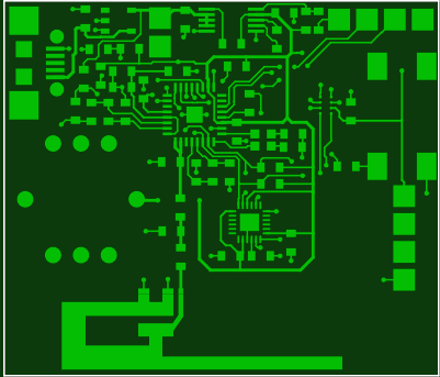
Hi there, I am a EE graduate student. I am designing a custom board using the CC2650. I have completed the schematic and the pcb design and I would like a review of my schematic and gerbers just to make sure I did everything right. This is indeed the first time I design a board. In particular, the RF part is what worries me more. The TA who followed me in the design recommended this scheme and routing but, according to the TRM and  what I've done appears to be different (with single-ended antenna, is it correct to short circuit RF_N and RF_P if I remove the inductance?).
Thank you in advance for your time,
Jackmicrocontroller_schematic.pdfbattery_management_schematic.pdfsensors_schematic.pdfpower_schematic.pdf