This thread has been locked.

If you have a related question, please click the "Ask a related question" button in the top right corner. The newly created question will be automatically linked to this question.

CC2640R2F: CC2640R2F 7x7 layout suggestions

Part Number: CC2640R2F

HI,

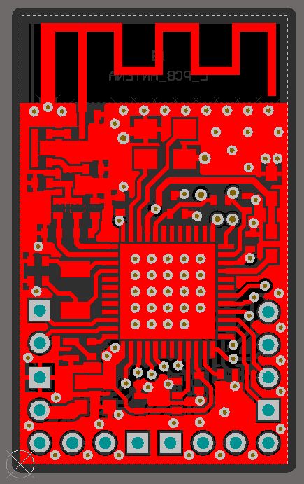
Could anybody have take a look on this layout ?

It is CC2640R2F in 48pin 7x7 package, 4 layer layout on 0.8mm pcb based on AN048 PCB antenna

I don't have possibility to follow precisely to reference RF path from LaunchPad

and since I don't have RF expertise it bothers me if components path

from  chip pins to antenna could be twisted that way?

maybye some other valuable suggestions ?

I am aware of CC26XX checklist and HW training layout.

Please answer to give valuable content to the forum

Thank You

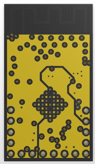
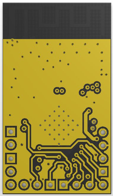
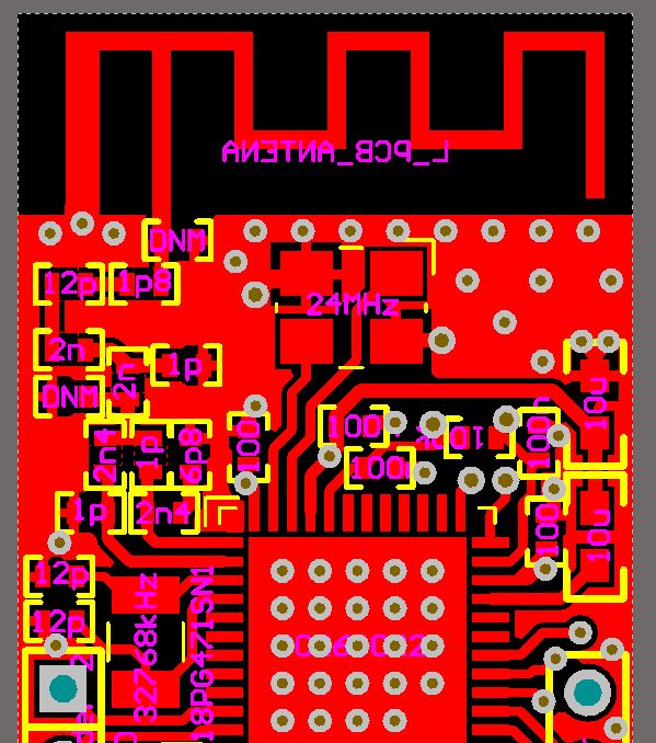
TOP LAYER
POWER PLANE
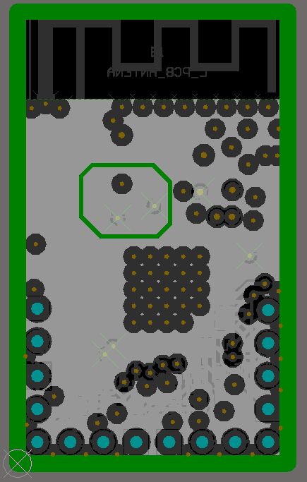
GND

BOTTOM LAYER

  • Hi Lukas,

    Asymmetrical traces from the RF_P/RF_N pins to the balun will possibly degrade the RF performance.

    We recommend to have the ground plane as layer #2 so that the RF traces on layer #1 have GND as reference plane. Looks like you have the power plane as layer #2?

    There should be some more GND vias surrounding the RF front-end. 

    To save space you can consider the 5x5 package, it looks like you don't need all the IOs of a 7x7 package?


    Best regards,
    Simon

  • Hi Simon,

    Thank You for Your answer.

    I delayed my reply until my layout is finished.

    I have adopted all hints You proposed and applied all

    recomendations suported by the TI (I am considering 5x5 package)

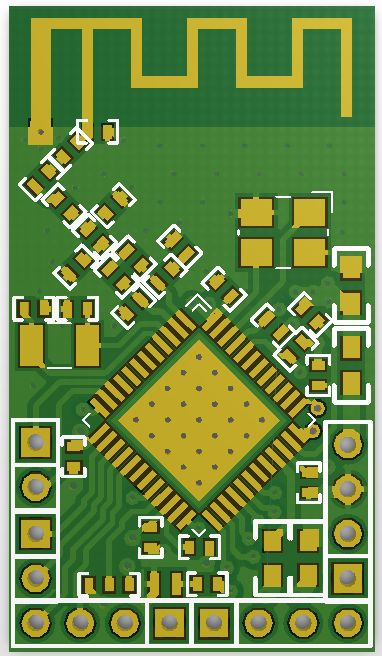
    I want to close my layout as shown.

    Before marking my post as solved,

    please once again take a look on it and write down all issues due to You can cause potential problems.

    What bothers me are angled bends at feed point to PCB antena but in defined shape i can not

    find better placement.

    3D View

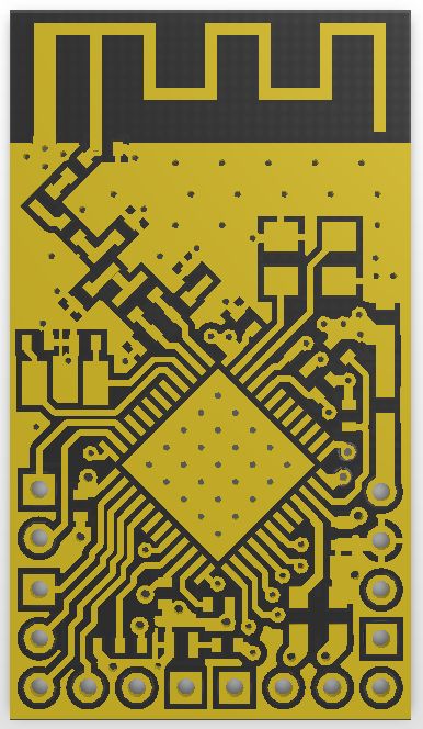
    Top Layer - copper view

    MID1 - GND Layer (below top layer)

    MID2 - power planes - VDDR and VDDS

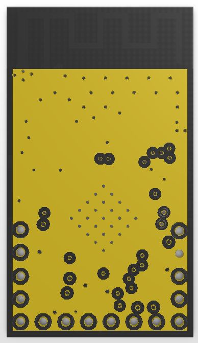
    Bottom Layer

    Thank You for Your time

  • Hi Lukas,

    This looks much better! Some comments:

    - The inductor and capacitor of the DCDC should be tied together on the top layer and not just through two vias to the VDDR power plane. You can remove the via on the inductor and make a direct connection to the capacitor.

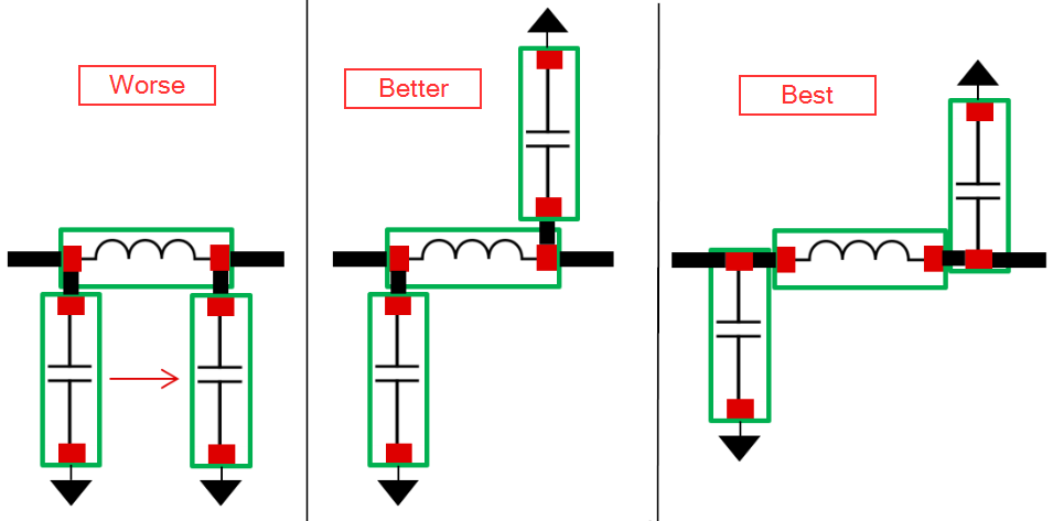
    - The pi filter can be improved by moving the capacitor pads inline with the RF trace. However, I think this will be difficult to accomplish on this layout. 

    Pi filter 

    Best regards,
    Simon

  • Thanks a lot
    indeed I have overlooked the inductor and capacitor of the DCDC direct connection.