- Ask a related questionWhat is a related question?A related question is a question created from another question. When the related question is created, it will be automatically linked to the original question.
Tool/software: Code Composer Studio
Using two CC2640 LAUNCHPAD , serve as SPI SLAVE & SPI MASTER respectively . SPI MASTER writes data and SPI SALVE reads data . However , when SPI SLAVE reads data , only the first byte that SPI MASTER writes can be read , during the state of SPI CSN keeping at the low level . Where am I wrong when configuring the SPI CSN ?
1. configuration of SPI SLAVE
(1)SPI GPIO configuration
#define CC2640R2_LAUNCHXL_SPI0_MISO             IOID_6          /* RF1.20 */
#define CC2640R2_LAUNCHXL_SPI0_MOSI             IOID_7          /* RF1.18 */
#define CC2640R2_LAUNCHXL_SPI0_CLK              IOID_10         /* RF1.16 */
#define CC2640R2_LAUNCHXL_SPI0_CSN              IOID_20
(2)BoardGpioInitTable
const PIN_Config BoardGpioInitTable[] = {

    CC2640R2_LAUNCHXL_PIN_RLED | PIN_GPIO_OUTPUT_EN | PIN_GPIO_LOW | PIN_PUSHPULL | PIN_DRVSTR_MAX,       /* LED initially off */
    CC2640R2_LAUNCHXL_PIN_GLED | PIN_GPIO_OUTPUT_EN | PIN_GPIO_LOW | PIN_PUSHPULL | PIN_DRVSTR_MAX,       /* LED initially off */
    CC2640R2_LAUNCHXL_PIN_BTN1 | PIN_INPUT_EN | PIN_PULLUP | PIN_IRQ_BOTHEDGES | PIN_HYSTERESIS,          /* Button is active low */
    CC2640R2_LAUNCHXL_PIN_BTN2 | PIN_INPUT_EN | PIN_PULLUP | PIN_IRQ_BOTHEDGES | PIN_HYSTERESIS,          /* Button is active low */
    //CC2640R2_LAUNCHXL_SPI_FLASH_CS | PIN_GPIO_OUTPUT_EN | PIN_GPIO_HIGH | PIN_PUSHPULL | PIN_DRVSTR_MIN,  /* External flash chip select */
    CC2640R2_LAUNCHXL_UART_RX | PIN_INPUT_EN | PIN_PULLDOWN,                                              /* UART RX via debugger back channel */
    /*-----当不使用UART时,应该将UART TX拉低,避免漏电 -----*/
    CC2640R2_LAUNCHXL_UART_TX | PIN_GPIO_OUTPUT_EN | PIN_GPIO_LOW | PIN_PUSHPULL,
    /*CC2640R2_LAUNCHXL_UART_TX | PIN_GPIO_OUTPUT_EN | PIN_GPIO_HIGH | PIN_PUSHPULL,*/                    /* UART TX via debugger back channel */

    CC2640R2_LAUNCHXL_SPI0_MOSI | PIN_INPUT_EN | PIN_PULLDOWN,                                            /* SPI master out - slave in */
    CC2640R2_LAUNCHXL_SPI0_MISO | PIN_GPIO_OUTPUT_EN | PIN_GPIO_HIGH | PIN_PUSHPULL,                       /* SPI master in - slave out */
    CC2640R2_LAUNCHXL_SPI0_CLK | PIN_INPUT_EN | PIN_PULLDOWN,                                             /* SPI clock */
    CC2640R2_LAUNCHXL_SPI0_CSN | PIN_BM_INPUT_EN | PIN_PULLDOWN,

    /*-----这里的配置是多余的,在ccfg.c中配置bootloader back door就足够 -----*/
    /*BOOTLOADER_BACKDOOR | PIN_GPIO_OUTPUT_EN | PIN_GPIO_HIGH,*/

    PIN_TERMINATE
};
(3)SPI_init
static void Spi_task_init(void)
{
SPI_init(); // Initialize the SPI driver
// Init SPI and specify non-default parameters
SPI_Params_init(¶ms);
params.bitRate = 1000000;
params.dataSize = 8; // 8-bit data size
params.frameFormat = SPI_POL0_PHA0;
params.mode = SPI_SLAVE;
params.transferMode= SPI_MODE_BLOCKING;
// Open the SPI and perform the transfer
handle = SPI_open(Board_SPI0, ¶ms);
}(4)SPI read
uint8_t frame_total_dummy[32]  = { 0x00,0x00,0x00,0x00,0x00,0x00,0x00,0x00,0x00,0x00,
                                   0x00,0x00,0x00,0x00,0x00,0x00,0x00,0x00,0x00,0x00,
                                   0x00,0x00,0x00,0x00,0x00,0x00,0x00,0x00,0x00,0x00,
                                   0x00,0x00};

uint8_t SPI_transfer_frame_read(SPI_Handle handle, SPI_Transaction *transaction)
{
    uint8_t uint8t_ret = 0;
    bool bool_ret = true;

    transaction->count = 32;
    transaction->rxBuf = &frame_total_dummy[0];
    transaction->txBuf = NULL;

    bool_ret = SPI_transfer(handle, transaction);
    if(bool_ret == false)
    {
        return 0;
    }

    return uint8t_ret;
}
2. configuration of SPI MASTER
(1)SPI GPIO configuration
#define CC2640R2_LAUNCHXL_SPI0_MISO             IOID_6          /* RF1.20 */
#define CC2640R2_LAUNCHXL_SPI0_MOSI             IOID_7          /* RF1.18 */
#define CC2640R2_LAUNCHXL_SPI0_CLK              IOID_10         /* RF1.16 */
#define CC2640R2_LAUNCHXL_SPI0_CSN              IOID_20 //PIN_UNASSIGNED
(2)BoardGpioInitTable
const PIN_Config BoardGpioInitTable[] = {

    CC2640R2_LAUNCHXL_PIN_RLED | PIN_GPIO_OUTPUT_EN | PIN_GPIO_LOW | PIN_PUSHPULL | PIN_DRVSTR_MAX,       /* LED initially off */
    CC2640R2_LAUNCHXL_PIN_GLED | PIN_GPIO_OUTPUT_EN | PIN_GPIO_LOW | PIN_PUSHPULL | PIN_DRVSTR_MAX,       /* LED initially off */
    CC2640R2_LAUNCHXL_PIN_BTN1 | PIN_INPUT_EN | PIN_PULLUP | PIN_IRQ_BOTHEDGES | PIN_HYSTERESIS,          /* Button is active low */
    CC2640R2_LAUNCHXL_PIN_BTN2 | PIN_INPUT_EN | PIN_PULLUP | PIN_IRQ_BOTHEDGES | PIN_HYSTERESIS,          /* Button is active low */
    //CC2640R2_LAUNCHXL_SPI_FLASH_CS | PIN_GPIO_OUTPUT_EN | PIN_GPIO_HIGH | PIN_PUSHPULL | PIN_DRVSTR_MIN,  /* External flash chip select */
    CC2640R2_LAUNCHXL_UART_RX | PIN_INPUT_EN | PIN_PULLDOWN,                                              /* UART RX via debugger back channel */
    /*-----当不使用UART时,应该将UART TX拉低,避免漏电 -----*/
    CC2640R2_LAUNCHXL_UART_TX | PIN_GPIO_OUTPUT_EN | PIN_GPIO_LOW | PIN_PUSHPULL,
    /*CC2640R2_LAUNCHXL_UART_TX | PIN_GPIO_OUTPUT_EN | PIN_GPIO_HIGH | PIN_PUSHPULL,*/                    /* UART TX via debugger back channel */

    CC2640R2_LAUNCHXL_SPI0_MOSI| PIN_GPIO_OUTPUT_EN | PIN_GPIO_HIGH | PIN_PUSHPULL,                       /* SPI master out - slave in */
    CC2640R2_LAUNCHXL_SPI0_MISO| PIN_INPUT_EN | PIN_PULLDOWN,                                             /* SPI master in - slave out */
    CC2640R2_LAUNCHXL_SPI0_CLK | PIN_INPUT_EN | PIN_PULLDOWN,                                             /* SPI clock */
    CC2640R2_LAUNCHXL_SPI0_CSN | PIN_GPIO_OUTPUT_EN | PIN_GPIO_HIGH | PIN_PUSHPULL | PIN_DRVSTR_MIN,

    /*-----这里的配置是多余的,在ccfg.c中配置bootloader back door就足够 -----*/
    /*BOOTLOADER_BACKDOOR | PIN_GPIO_OUTPUT_EN | PIN_GPIO_HIGH,*/

    PIN_TERMINATE
};
(3)SPI_init
static void Spi_task_init(void)
{
SPI_init(); // Initialize the SPI driver
// Init SPI and specify non-default parameters
SPI_Params_init(¶ms);
params.bitRate = 1000000;
params.dataSize = 8; // 8-bit data size
params.frameFormat = SPI_POL0_PHA0;
params.mode = SPI_MASTER;
params.transferMode= SPI_MODE_BLOCKING;
// Open the SPI and perform the transfer
handle = SPI_open(Board_SPI0, ¶ms);
hPins = PIN_open(&SPI_CSN_PinState, SPI_CSN_PinTable);
interrupt_event_init();
mcu_msg_fifo_init();
}
(4)SPI read
uint8_t txBuffer[]  = { 0x5A ,0x5A ,0xA5 ,0xA5 ,0x01 ,0xFF ,0x00 ,0x16 ,0x33 ,0x44 ,
                        0x55 ,0x66 ,0x33 ,0x44 ,0x55 ,0x66 ,0x33 ,0x44 ,0x55 ,0x66 ,
                        0x33 ,0x44 ,0x55 ,0x66 ,0x33 ,0x44 ,0x55 ,0x66 ,0x33 ,0x44 ,
                        0x00 ,0xDB};

uint8_t SPI_transfer_frame_write(PIN_Handle pin_handle,SPI_Handle handle,SPI_Transaction *transaction,uint8_t *buffer, size_t size)
{
    uint8_t uint8t_ret = 0;
    bool bool_ret = true;

    transaction->count = size;
    transaction->txBuf = buffer;
    transaction->rxBuf = NULL;

    PIN_setOutputValue(pin_handle, CC2640R2_LAUNCHXL_SPI0_CSN_MANUAL, 0);

    bool_ret = SPI_transfer(handle, transaction);
    if(bool_ret == true)
    {
        uint8t_ret = 1;
    }
    else
    {
        uint8t_ret = 0;
    }

    PIN_setOutputValue(pin_handle, CC2640R2_LAUNCHXL_SPI0_CSN_MANUAL, 1);

    return uint8t_ret;

}

static void Spi_taskFxn(UArg a0, UArg a1)
{
  Spi_task_init();

  SPI_transfer_frame_write(handle, &transaction,txBuffer, 32);
}
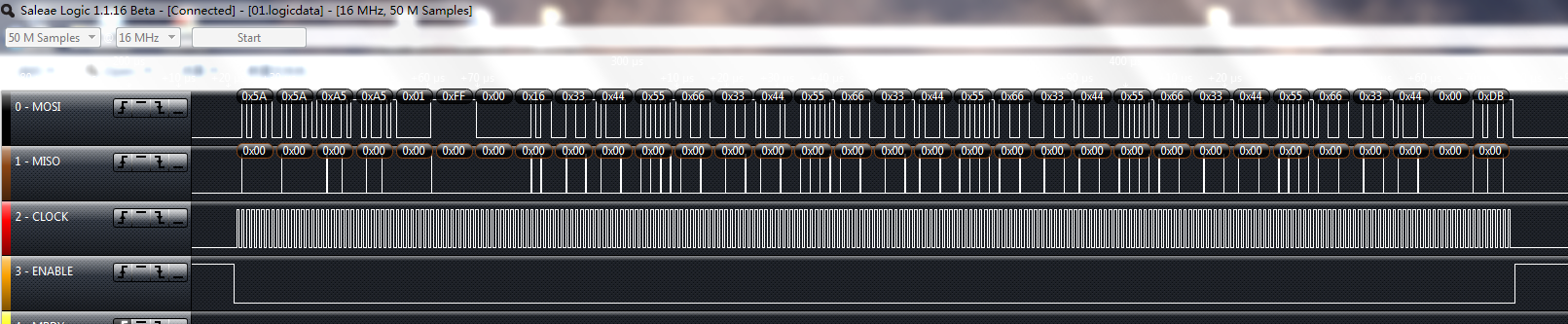
3.Using the configuration above , 32 bytes of data were written during the state of SPI CSN keeping at the low level ,as shown in picture 1.

picture 1
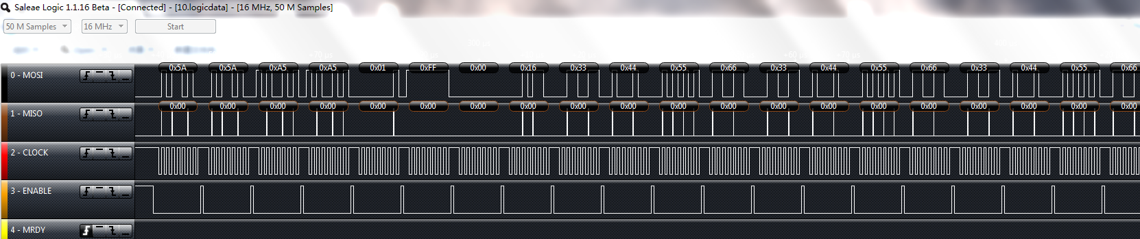
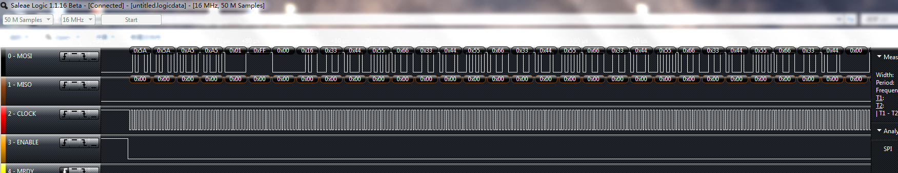
4.Connecting SPI MASTER and SPI SLAVE, as shown in picture 2 and picture 3.

picture2

picture 3
5.SPI SLAVE can read only the first byte----0X5A
6.If SPI MASTER using the default SPI CSN configuration , SPI SLAVE can read all the datas that SPI MASTER writes .SPI MASTER writes 32 bytes of data during the state of SPI CSN keeping at the low level , as shown in picture 4.

picture 4
Where am I wrong when configuring the SPI CSN ?
7.attachments
(1)simplelink_cc2640r2_sdk_1_40_00_45 can be downloaded here :
(2)CC2640R2 launchpad can be bought here:
8.my developing environment
CCS:Code Composer Studio 7.2.0
SDK:simplelink_cc2640r2_sdk_1_40_00_45
hardware:CC26640R2 launchpad develop kit
VS: Microsoft Visual C++ 2010 Express
OS:win7 64 bit