This thread has been locked.

If you have a related question, please click the "Ask a related question" button in the top right corner. The newly created question will be automatically linked to this question.

CC2541: Issue with Impedance Control and Antenna Tuning

Part Number: CC2541

Hello,

I am designing a custom board using following components:
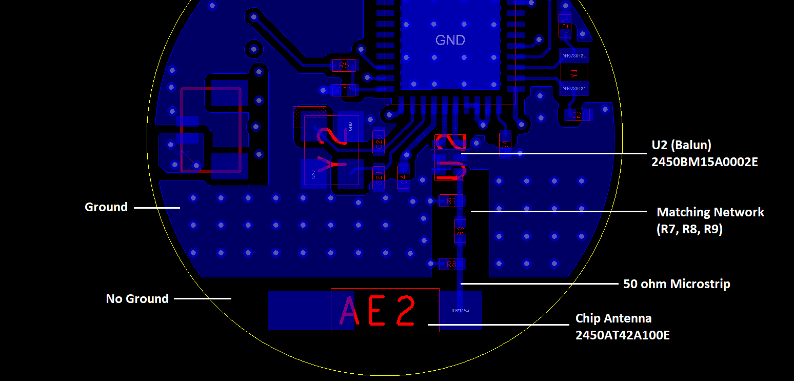
SoC: CC2541 
Balun: Johanson 2450BM15A0002E
Matching Network: R9(0ohm), R7(DNM), R8(DNM)
Chip Antenna: Johanson 2450AT42A100E

Layer 1: RF layer
Layer 2: Ground
Layer 3: Power
Layer 4: Bottom

The board is being designed with impedance(50 ohm) controlled track (Microstrip) as recommended in the datasheet of chip antenna without any matching network and TI's postage stamp. Below is the screenshot of my current design:


Below is my calculation for impedance:

For this design, I want to confirm from the experts on e2e, whether my design is go-ahead for production or not. Please let me know if there should be some modifications at any place to achieve maximum efficiency. 


Thank you,

Madhav


  • - The trace from R8 to the antenna is too short to act like a transmission line meaning it should be no issues there.
    - You should check with Johanson on the recommended minimum spacing from the antenna to the ground layer. The distance looks short which I suspect will cause loss in effectivity.
    - The two shunt components in the match should have a mode solid connection to ground.
  • Hello TER,

    Thank you for your reply. As mentioned by you in 2nd comment, Yes it was shorter than what was recommended by Johanson(1mm), so I have edited for the same.   

    I am still skeptical that the footprint of R7, R8 and R9 is wider than the track width. Also, the other pad(GND) of R7 and R8 is nearer to the track as compared to rest ground-track separation. Can you please comment on this? Won't it affect the 50 ohm characteristic impedance of the track or is it alright?

    Thank you,

    Madhav

  • I see in most of our reference designs we have done the traces between the components are as wide as the footprint. Not sure how much impact using wide vs narrow traces will have on the performance. For short traces use wide traces, for this layout from the IPC to the antenna.