Other Parts Discussed in Thread: CC2640
Hy,
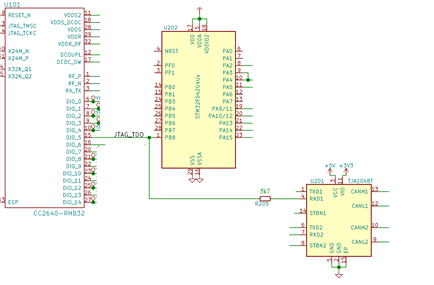
I am observing a very strange effect which I have no explanation for. I have the following schematic:
The DIO 5 (and DIO6) shall control the input pin of a 2nd controller (STM32) which is also controlled by an output of a bus transceiver. This is necessary because I need to control the state of the Pin PB8 during boot: It must be 0 during reset and be controlled by the bus transceiver during normal operation.
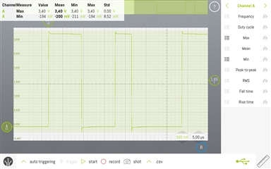
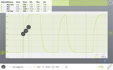
When I look at the signal left and right of the Resistor R205 I see some sort of a huge capacitance:
So the digital signal has a rise time of about 2.5us. There must be an input capacitance of some hundreds pF somewhere.
Is there any explanation in the CC2640 that could explain this issue? Do the JTAG pins behave in a special way? I do not use JTAG nor have I a debugger connected. How do I need to configure the pin to be high impedant / low capacitant?
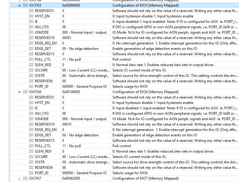
When I do connect my debugger and look into IO configuration I see the following:
Anything peculiar?
Best regards
Harald


