


Other Parts Discussed in Thread: CC2541, CC2540
art Number: CC2541
Hello,
I have gone through couple of threads on writing Flash memory.
Bit confused with 8051 CPU flash of 64K Bytes, CC2541 flash size of 256K bytes, Banks 0 - 7, Pages 0 - 127, Logical address, Actual/Physical address, 32K Flash occupying XDATA etc..
User guide is not clear about mapping. Below are the links I was going through.
http://e2e.ti.com/support/wireless-connectivity/bluetooth/f/538/t/319364
https://e2e.ti.com/support/wireless-connectivity/sub-1-ghz/f/156/p/279926/977092#977092
Is there any table mapping between all these.
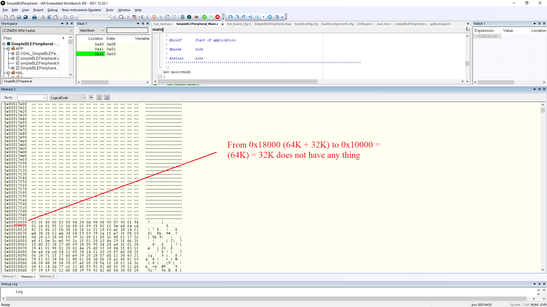
I was going through IAR memory map.
There is a gap between first 64K and next 32K. Later on every alternative 32K does not have code. Why is this. Trying to understand the concept behind this.

Thanks & Regards
Vishnu Beema

