Other Parts Discussed in Thread: CC2640R2F
Team,
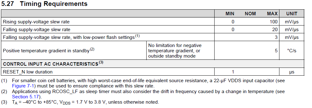
My customer who employs the CC2640R2F-Q1 would like to know the timing requirement of rising pin - VDDR/VDDR_RF/VDDS/VDDS2/VDDS3/VDDS_DCDC/...
The VDDx pins on their board would connect with difference decoupling cap each other. So the rising time of each are a bit difference during power-up. I glanced over the data sheet. It tells that we define only skew rate. Do we have strict rule when power-up sequence for the VDDx pins?
Regards,
Nonaka


