This thread has been locked.

If you have a related question, please click the "Ask a related question" button in the top right corner. The newly created question will be automatically linked to this question.

BOOSTXL-AOA: About PCB pattern

Part Number: BOOSTXL-AOA

Hello, 

I have some questions about the PCB pattern of BOOSTXL-AOA Booster Pack. 

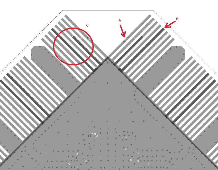
There are GND patterns on Layer2 and 5. Please see the attached image file. 

1. Regarding the part is indicated by arrows (A), what is a function of Resistor? 

2. Regarding the pattern is indicated by arrows (B), why it is dark color than other pattern? 

3. Regarding the part is circled (C), why these GND pattern are comb line shape? 

Please advise. 

Shoko 

  • Hi Shoko,

    1. The function of the resistor is to dissipate any RF energy that can occur in the ground finger so that it's not re-radiated to the nearest parallel dipole antenna.
    2. No reason, they should all have the same color. If you look at the Gerber files you'll see that there no difference.
    3. Same reason as for question 1 (avoid re-radiation to the nearest parallel dipole antenna)

    Best Regards,
    R.M