This thread has been locked.

If you have a related question, please click the "Ask a related question" button in the top right corner. The newly created question will be automatically linked to this question.

CC2564C: CC2564C output power modification in EDR

Part Number: CC2564C
Other Parts Discussed in Thread: WL1833,

Hi,

I'm trying to tune EDR output power in bts file.

my setting is shown below:

#Set BT BR (GFSK) LP Vectors Values (note the need to multiply the output power in dBm by '2')
Send_HCI_VS_DRPb_Set_Power_Vector 0xFD82, 0x00, 0x14, 0xbb, 0xbb, 0xbb, 0xbb, 0xbb, 0xbb, 0xbb, 0xbb, 0xc6, 0xd1, 0xdc, 0xe7, 0xf2, 0xfd, 0x08, 0xff, 0x0000
Wait_HCI_Command_Complete_VS_DRPb_Set_Power_Vector_Event 5000, 0x00, 0xfd82, 0x00

#Set BT BR EDR 2MB LP Vectors Values (note the need to multiply the output power in dBm by '2')
Send_HCI_VS_DRPb_Set_Power_Vector 0xFD82, 0x01, 0x9c, 0xbb, 0xbb, 0xbb, 0xbb, 0xbb, 0xbb, 0xbb, 0xbb, 0xc6, 0xd1, 0xdc, 0xe7, 0xf2, 0xfd, 0x08, 0xff, 0x0000
Wait_HCI_Command_Complete_VS_DRPb_Set_Power_Vector_Event 5000, 0x00, 0xfd82, 0x00

#Set BT BR EDR 3MB LP Vectors Values (note the need to multiply the output power in dBm by '2')
Send_HCI_VS_DRPb_Set_Power_Vector 0xFD82, 0x02, 0x9c, 0xbb, 0xbb, 0xbb, 0xbb, 0xbb, 0xbb, 0xbb, 0xbb, 0xc6, 0xd1, 0xdc, 0xe7, 0xf2, 0xfd, 0x08, 0xff, 0x0000

From BT tester, TP/TRM/CA/BV-10-C (EDR Relative Transmit Power) will be tested in EUT Max and EUT Min.

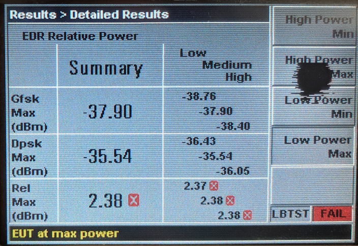
Under this setting , difference of EUT MAX is pass but difference of EUT MIN is always margin failed.

Is there any advice on tuning this parameter?

Best,

Kevin 

  • Kevin,

    Could you please share the test results where the EUT MIN fails? 

    Best regards,

    Vihang

  • Hi Vihang,

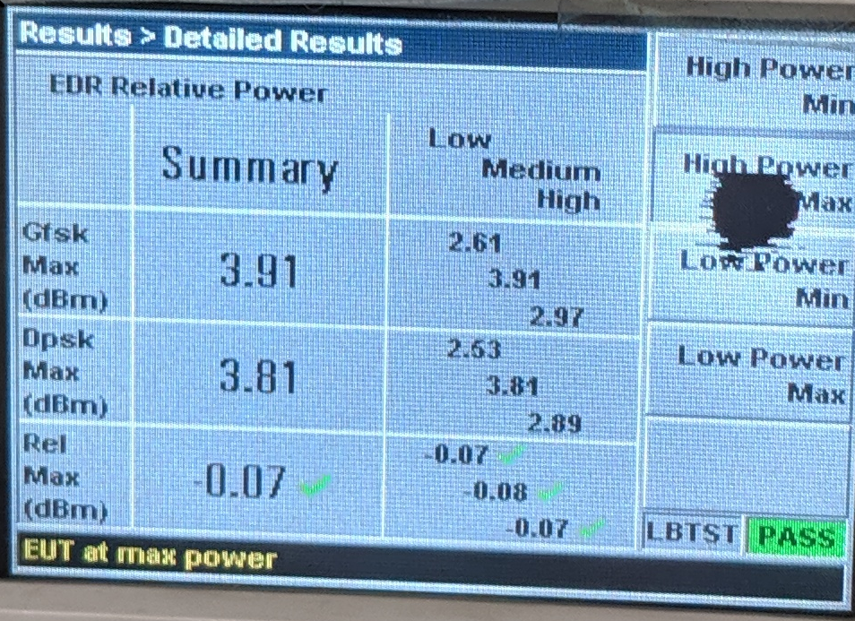
    for the result is shown below:

    DUT at Min. Level:

    DUT at Max. Level:

    specification for EDR relative power is (P GFSK  - 4dB) < P DPSK  < (P GFSK  + 1dB)

    I think DUT at Max. Level has enough buffer for the Spec but  DUT at Max. doesn't.

    i tried to modify power level 0 or 8 in 2MB table, but not help.

    Best,

    Kevin 

  • Hi Vihang,

    here is what I experiment:

    #1 ERD power = BR value + 2

    #Set BT BR (GFSK) LP Vectors Values (note the need to multiply the output power in dBm by '2')
    Send_HCI_VS_DRPb_Set_Power_Vector 0xFD82, 0x00, 0x14, 0xbb, 0xbb, 0xbb, 0xbb, 0xbb, 0xbb, 0xbb, 0xbb, 0xc6, 0xd1, 0xdc, 0xe7, 0xf2, 0xfd, 0x08, 0xff, 0x0000
    Wait_HCI_Command_Complete_VS_DRPb_Set_Power_Vector_Event 5000, 0x00, 0xfd82, 0x00

    #Set BT BR EDR 2MB LP Vectors Values (note the need to multiply the output power in dBm by '2')
    Send_HCI_VS_DRPb_Set_Power_Vector 0xFD82, 0x01, 0x9c, 0xbd, 0xbd, 0xbd, 0xbd, 0xbd, 0xbd, 0xbd, 0xbd, 0xc8, 0xd3, 0xde, 0xe9, 0xf5, 0xff, 0x0a, 0xff, 0x0000
    Wait_HCI_Command_Complete_VS_DRPb_Set_Power_Vector_Event 5000, 0x00, 0xfd82, 0x00

    #Set BT BR EDR 3MB LP Vectors Values (note the need to multiply the output power in dBm by '2')
    Send_HCI_VS_DRPb_Set_Power_Vector 0xFD82, 0x02, 0x9c, 0xbd, 0xbd, 0xbd, 0xbd, 0xbd, 0xbd, 0xbd, 0xbd, 0xc8, 0xd3, 0xde, 0xe9, 0xf5, 0xff, 0x0a, 0xff, 0x0000
    Wait_HCI_Command_Complete_VS_DRPb_Set_Power_Vector_Event 5000, 0x00, 0xfd82, 0x00

    #2 ERD power = BR value + 4

    Send_HCI_VS_DRPb_Set_Power_Vector 0xFD82, 0x00, 0x14, 0xbb, 0xbb, 0xbb, 0xbb, 0xbb, 0xbb, 0xbb, 0xbb, 0xc6, 0xd1, 0xdc, 0xe7, 0xf2, 0xfd, 0x08, 0xff, 0x0000
    Wait_HCI_Command_Complete_VS_DRPb_Set_Power_Vector_Event 5000, 0x00, 0xfd82, 0x00

    #Set BT BR EDR 2MB LP Vectors Values (note the need to multiply the output power in dBm by '2')
    Send_HCI_VS_DRPb_Set_Power_Vector 0xFD82, 0x01, 0x9e, 0xbf, 0xbf, 0xbf, 0xbf, 0xbf, 0xbf, 0xbf, 0xbf, 0xca, 0xd5, 0xdf, 0xeb, 0xf6, 0x01, 0x0c, 0xff, 0x0000
    Wait_HCI_Command_Complete_VS_DRPb_Set_Power_Vector_Event 5000, 0x00, 0xfd82, 0x00

    #Set BT BR EDR 3MB LP Vectors Values (note the need to multiply the output power in dBm by '2')
    Send_HCI_VS_DRPb_Set_Power_Vector 0xFD82, 0x02, 0x9e, 0xbf, 0xbf, 0xbf, 0xbf, 0xbf, 0xbf, 0xbf, 0xbf, 0xca, 0xd5, 0xdf, 0xeb, 0xf6, 0x01, 0x0c, 0xff, 0x0000

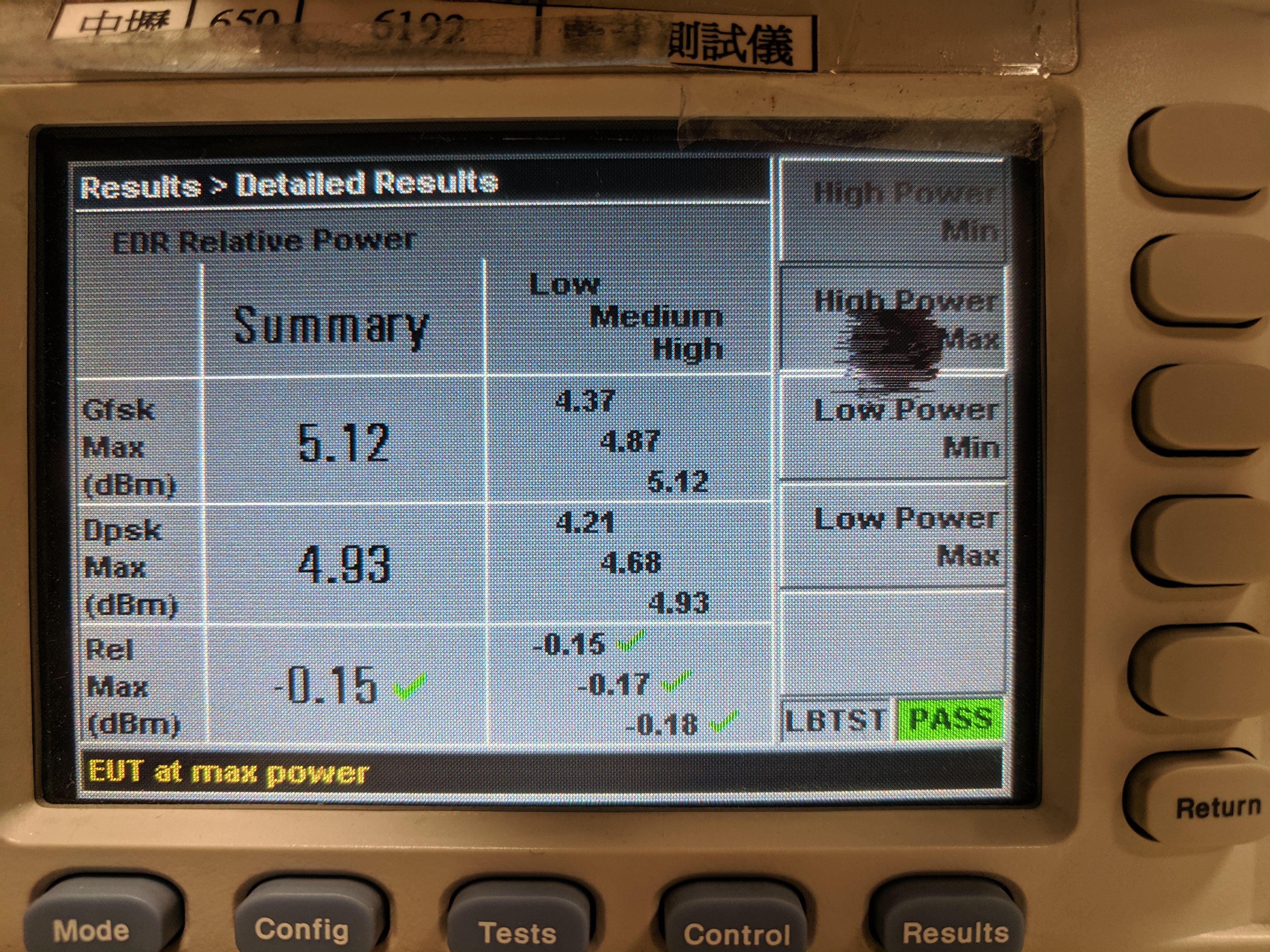
    In the first modification, the difference in DUT at Min. Level is pass.
    result is shown below:

    but in second modification, the test result is still the same with #1. I'm wondering whether experiment#1 is the best setting.

  • Kevin,

    Sorry for the delay.

    Typically, the max EDR power is kept several dB less than the max GFSK output power. Additionally, I also noticed a large step size in your settings that might be responsible for such failure. 

    Please start with the following settings and reduce each step, half a dB at a time, if needed for certification.

    # RF power tables for CC2564C QFN
    Send_HCI_VS_DRPb_Set_Power_Vector 0xFD82, 0x00, 0x9c, 0x18, 0xdc, 0xdc, 0xdc, 0xdc, 0xdc, 0xdc, 0xdc, 0xdc, 0xe6, 0xf0, 0xfa, 0x04, 0x0e, 0x18, 0xff, 0x0000
    Wait_HCI_Command_Complete_VS_DRPb_Set_Power_Vector_Event 5000, 0x00, 0xfd82, 0x00
    
    Send_HCI_VS_DRPb_Set_Power_Vector 0xFD82, 0x01, 0x9c, 0xd4, 0xd4, 0xd4, 0xd4, 0xd4, 0xd4, 0xd4, 0xd4, 0xd4, 0xdd, 0xe6, 0xef, 0xf8, 0x01, 0x0b, 0xff, 0x0000
    Wait_HCI_Command_Complete_VS_DRPb_Set_Power_Vector_Event 5000, 0x00, 0xfd82, 0x00
    
    Send_HCI_VS_DRPb_Set_Power_Vector 0xFD82, 0x02, 0x9c, 0xd4, 0xd4, 0xd4, 0xd4, 0xd4, 0xd4, 0xd4, 0xd4, 0xd4, 0xdd, 0xe6, 0xef, 0xf8, 0x01, 0x0b, 0xff, 0x0000
    Wait_HCI_Command_Complete_VS_DRPb_Set_Power_Vector_Event 5000, 0x00, 0xfd82, 0x00
    
    # Set Class 2 power
    Send_HCI_VS_DRPb_Set_Class2_Single_Power 0xFD87, 0x0d, 0x0e, 0x0e
    Wait_HCI_Command_Complete_VS_DRPb_Set_Class2_Single_Power_Event 5000, 0x00, 0xfd87, 0x00
    
    # Run TPC (Transmission Power Control) calibration
    Send_HCI_VS_DRPb_Enable_RF_Calibration 0xFD80, 0x00, 0x00000800, 0x01
    Wait_HCI_Command_Complete_VS_DRPb_Enable_RF_Calibration_Event 5000, 0x00, 0xfd80, 0x00

    Best regards,

    Vihang

  • Hi Vihang,

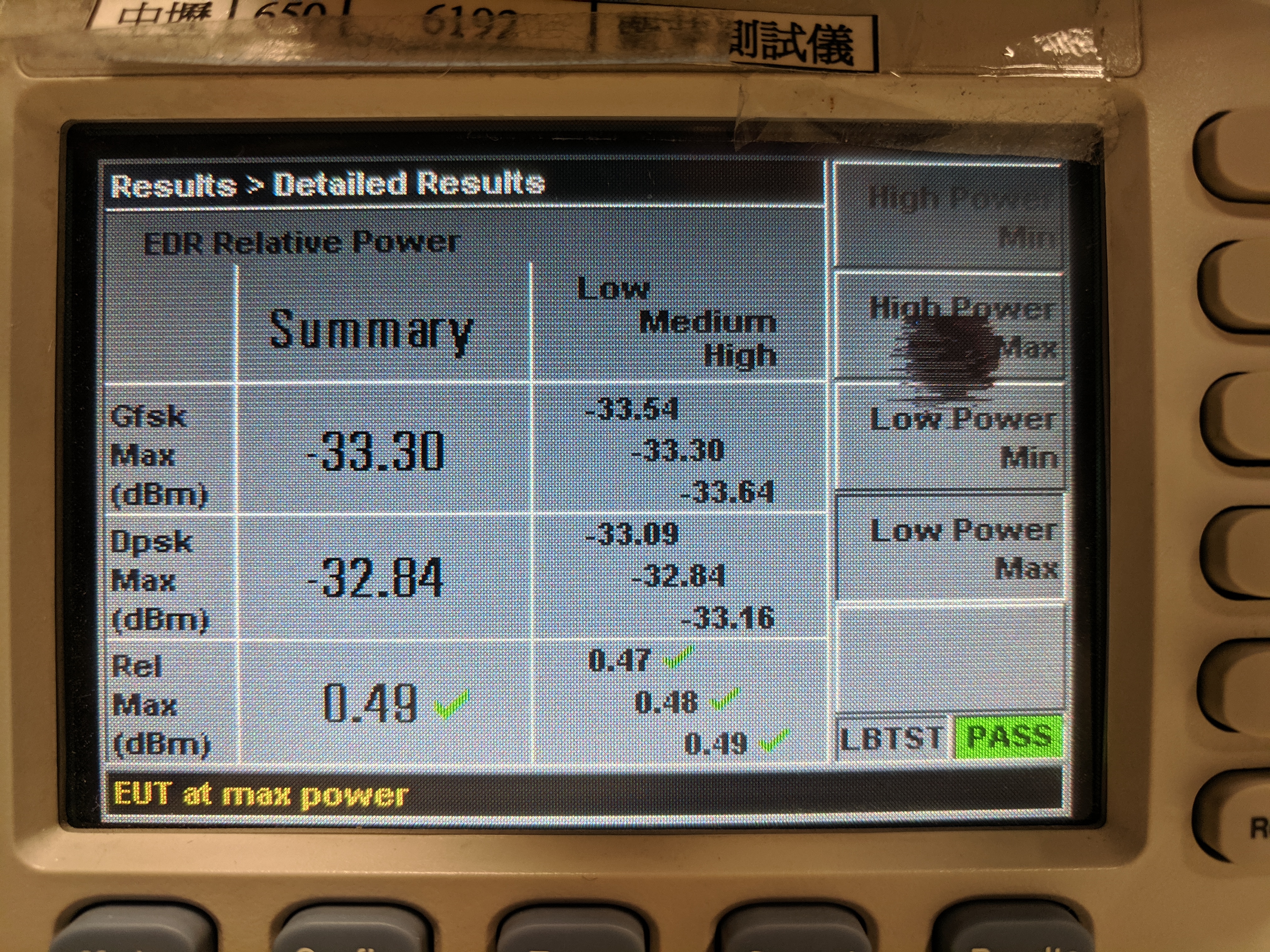
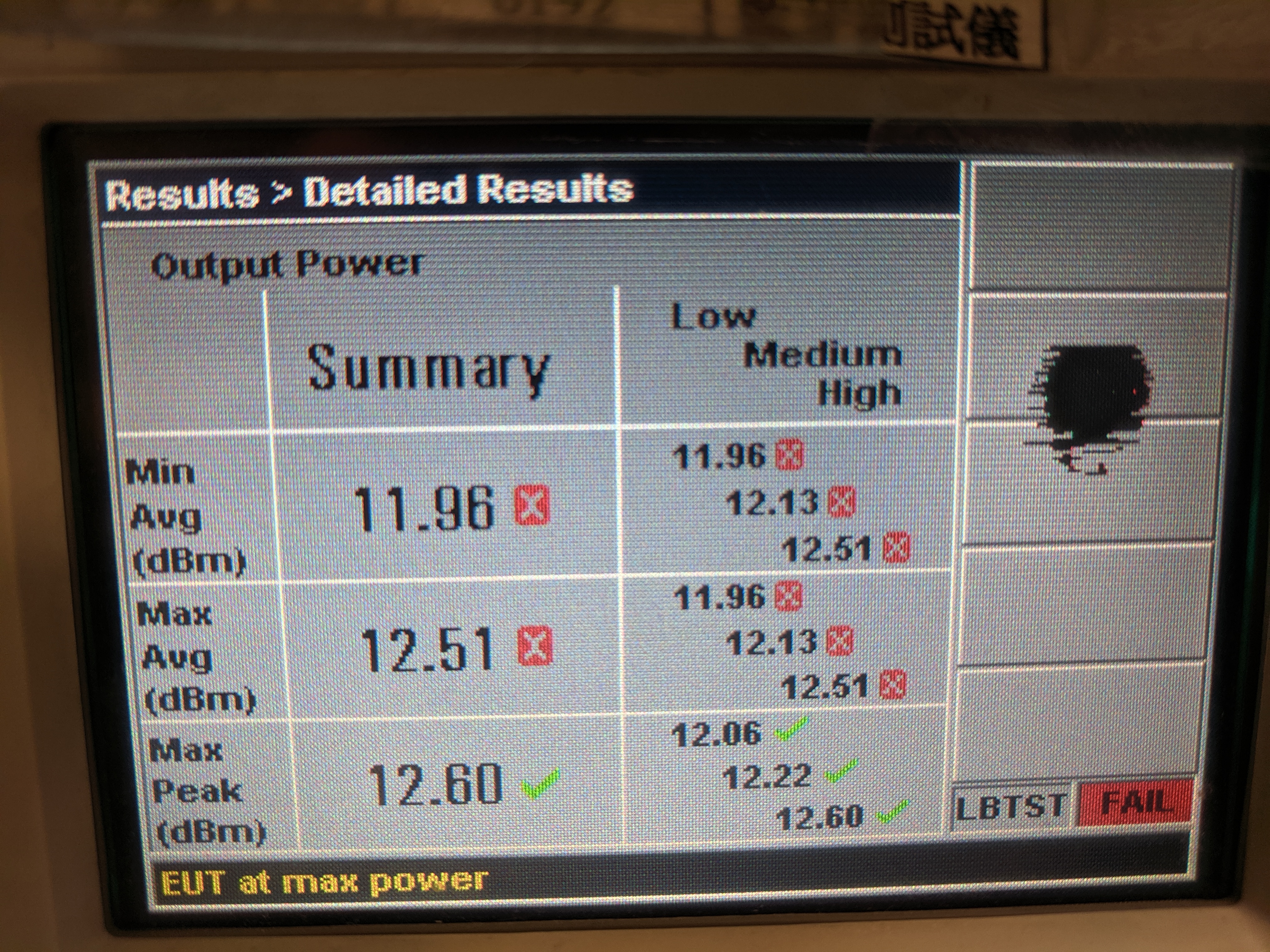
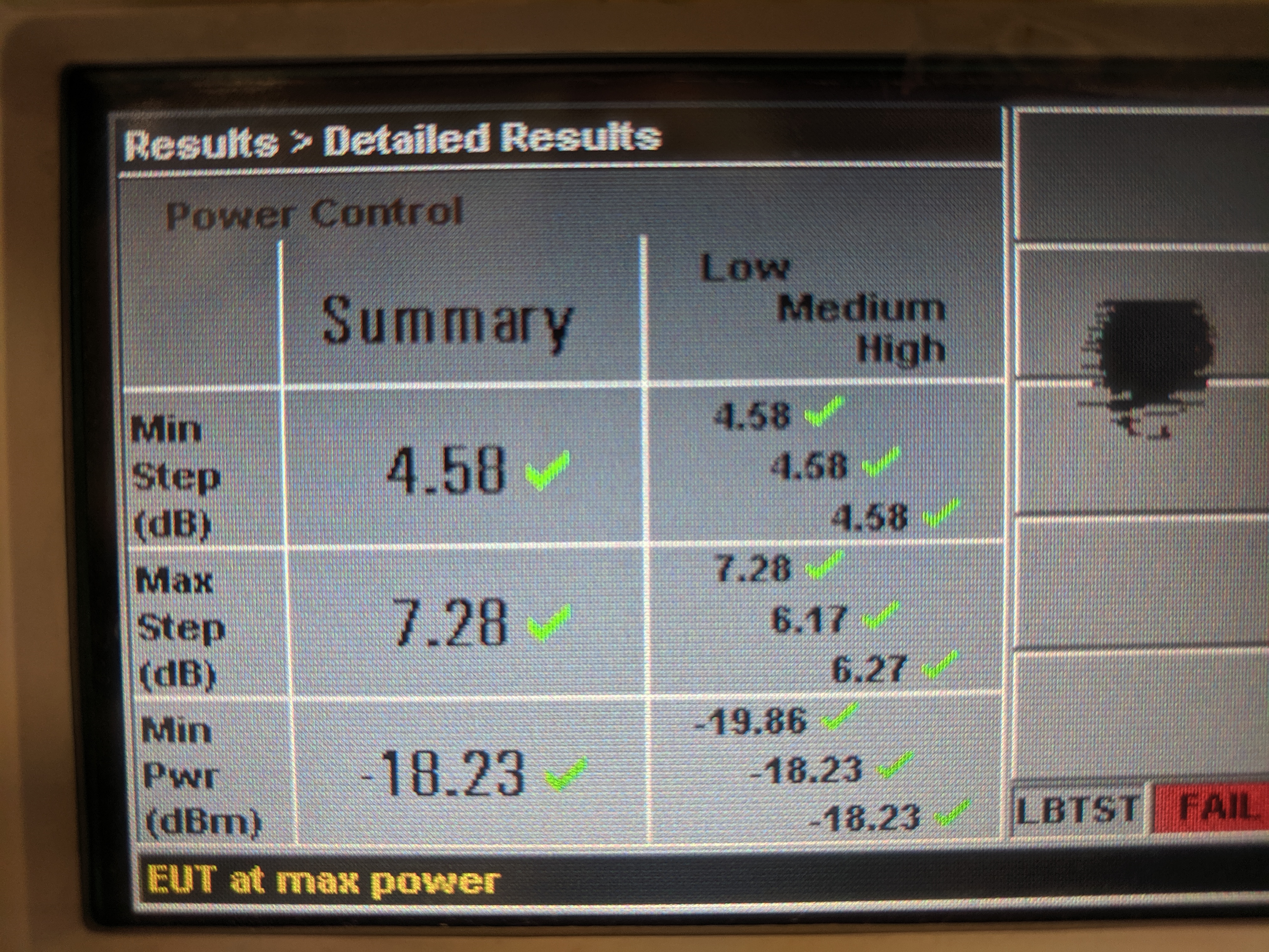
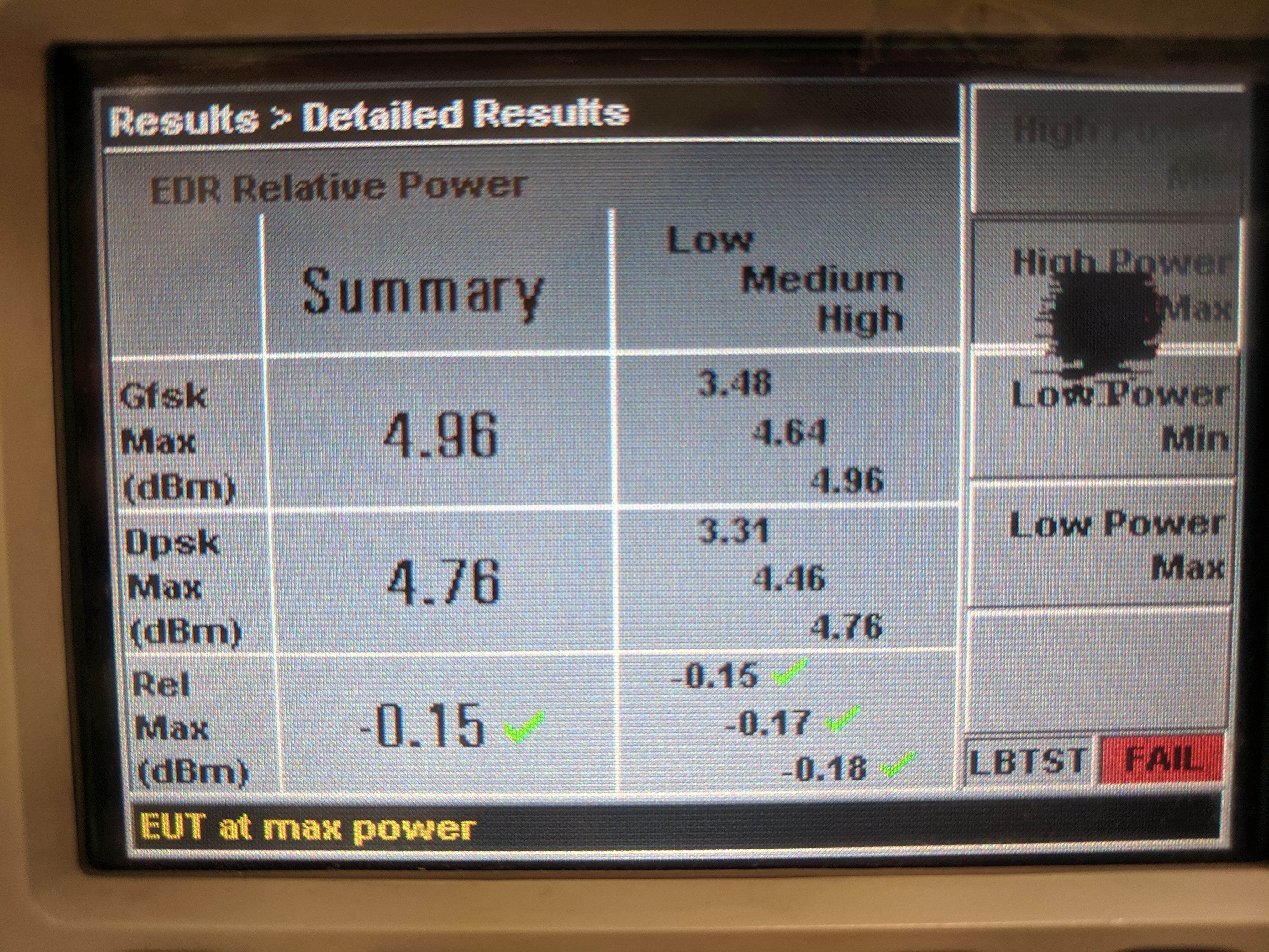
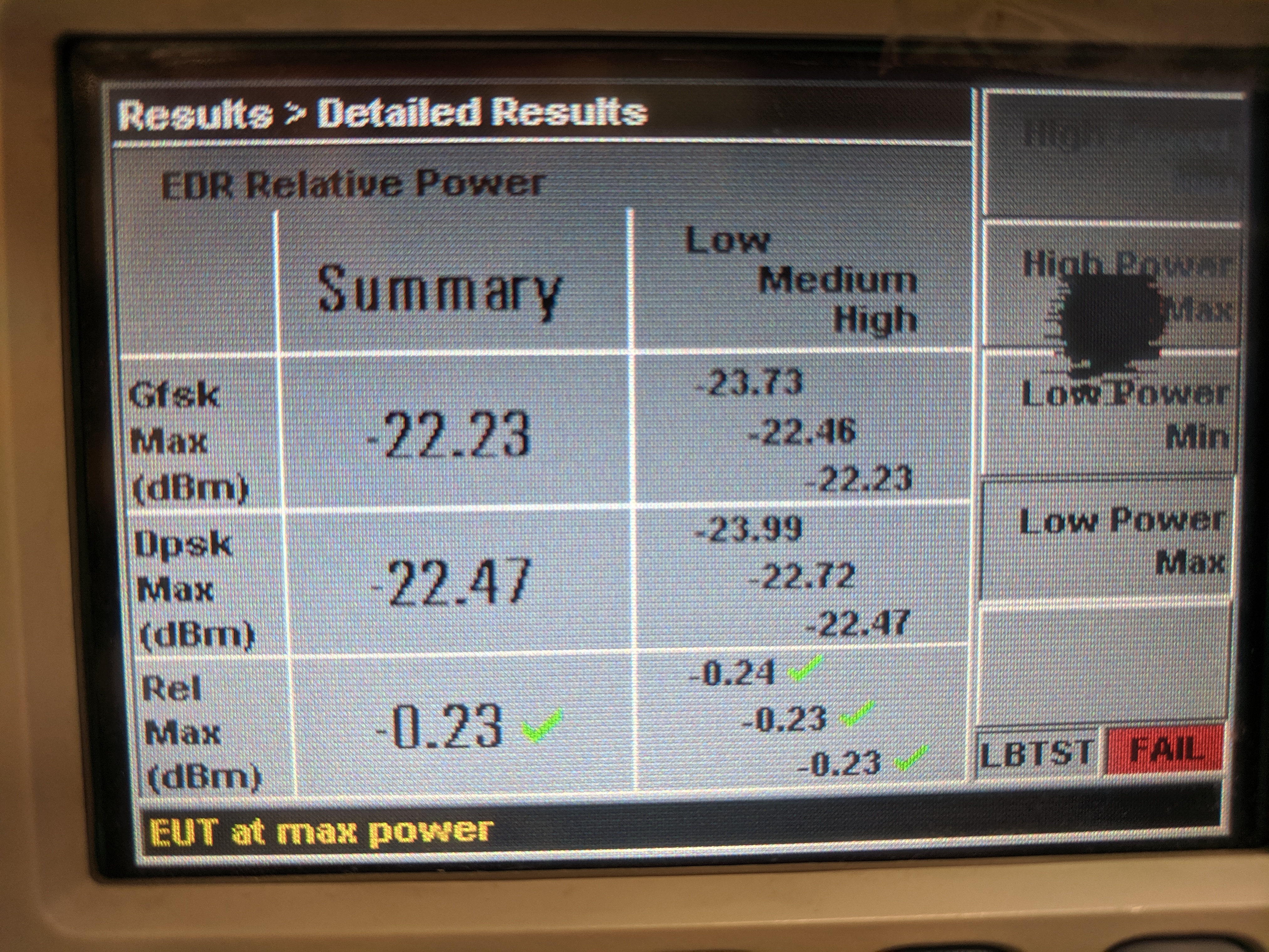
    I retest the item with new parameter you provide, and the results get better although output power is too large.(shown as below)

    output power for BR(GFSK)

    power control for BR

    EDR relative power (Max difference for high power) 

    EDR relative power (Max difference for low power) 

    then I'm going to decrease output power to meet my application, but I still have some question of the parameter.

    1. Is the output power in BR around 12 dBm defined by power level 15 value in "Send_HCI_VS_DRPb_Set_Power_Vector" ( real power value*2 and convert in Hexadecimal)? so,in EDR 2MB, maximum output power is around 5.5 dbm (0x0b) ?

    2. Does power control result come from the difference  between each the GFSK power level value of Send_HCI_VS_DRPb_Set_Power_Vector?

    3. In TP/TRM/CA-10-C, EDR relative power is define as "(P GFSK  - 4dB) < P DPSK  < (P GFSK  + 1dB)". Doesn't that mean the difference is between same power level setting ?(e.g.  result = (power level 15 value of GFSK) - (power level 15 value of DPSK))

    4. if I want to decrease BT output power to meet Bluetooth power class 2, should I subtract  a constant for every power level value in three Send_HCI_VS_DRPb_Set_Power_Vector or I just modify Send_HCI_VS_DRPb_Set_Class2_Single_Power?

    5. In chip WL1833, does it keep the same dB less between the max EDR power and the max GFSK output power for BT setting?

    Best,

    Kevin   

  • Hi Kevin,

    kevin Lin said:
    1. Is the output power in BR around 12 dBm defined by power level 15 value in "Send_HCI_VS_DRPb_Set_Power_Vector" ( real power value*2 and convert in Hexadecimal)? so,in EDR 2MB, maximum output power is around 5.5 dbm (0x0b) ?

    That is correct.

    kevin Lin said:
    2. Does power control result come from the difference  between each the GFSK power level value of Send_HCI_VS_DRPb_Set_Power_Vector?

    Yes.

    kevin Lin said:
    3. In TP/TRM/CA-10-C, EDR relative power is define as "(P GFSK  - 4dB) < P DPSK  < (P GFSK  + 1dB)". Doesn't that mean the difference is between same power level setting ?(e.g.  result = (power level 15 value of GFSK) - (power level 15 value of DPSK))

    The test spec refers to the average power. Due to the PAPR difference between the two modulations, the 12dBm and 5.5dBm peak powers are still within spec. To be on the safe side, you can lower just the GFSK power accordingly (all power levels as mentioned below).

    kevin Lin said:
    4. if I want to decrease BT output power to meet Bluetooth power class 2, should I subtract  a constant for every power level value in three Send_HCI_VS_DRPb_Set_Power_Vector or I just modify Send_HCI_VS_DRPb_Set_Class2_Single_Power?

    You need to subtract the constant from every power level in the power vector.

    The purpose of the HCI_VS_DRPb_Set_Class2_Single_Power command is to define the power level to be used if the remote side does not support the power control feature. According to the core spec, the controller should use class 2 or less power when the remote side does not support power control. In my example above, the highest power level for each modulation types that are less than 4dBm (max class 2 power) are picked from the power vectors for the HCI_VS_DRPb_Set_Class2_Single_Power command. If you modify the power vectors, you need to revise the HCI_VS_DRPb_Set_Class2_Single_Power setting accordingly.

    kevin Lin said:
    5. In chip WL1833, does it keep the same dB less between the max EDR power and the max GFSK output power for BT setting?

    The WL18xx devices have different output power and power vectors than CC2564C. Please refer to the SWRU442 for details regarding WL18xx devices.

    Best regards,

    Vihang