Part Number: CC2564C
Hi team,
I have questions from customer:
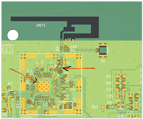
we are using the bluetooth module CC2564C but we have some routing problems:
1) Referring to SWRA420B.pdf document “CC2564x PCB Guidelines”, fig.6 /page6 shows the RF signal path from device pad B8 to decoupling C31 : well, I’m sorry buit we cannot follow your evaluation board routing because of the presence of local fiducial.
So, can we have problems if the routing between C31 and FL1 is a short linear connection? Please can you verify our routing solution below?
first image I attached before is from gerber files.
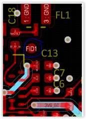
the next one is from PCB Guidelines.
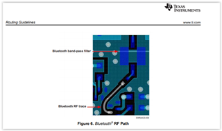
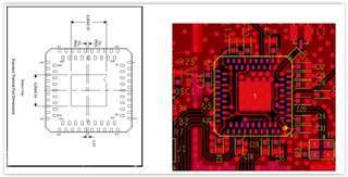
2)Figure14 shows the path starting from C25 to pad B15 and then to B26 and B27 on the other device side: it seems on top layer without vias, but this is not possible because of clearance constrain between centerpad of CC2564x. This because comparing the reference gerber file and datasheet the centerpad offset in gerber file is on the right side but in the datasheet is on the left side on top view. So, can we route with vias and without problem? What about this difference?
figure 14 refers to the previous document and the attached pictures are from datasheet and gerber.
Thanks,
Best regards,