This thread has been locked.

If you have a related question, please click the "Ask a related question" button in the top right corner. The newly created question will be automatically linked to this question.

CC Debugger schematic + firmware

Other Parts Discussed in Thread: CC2545, CC2592, CC2538, CC2543

Hi!

  is it possible to get the schematics and the firmware of the CC Debugger? We want to build that debugger ourself. We want to use it for a lab exercise.

Thank you very much!

Regards

Walter

  • Hi Walter,

    Both the schematics and firmware for CC debugger is already available online. You can find the schematics for the CC Debugger in the CC debugger User's guide (swru197), Section 10. The CC debugger firmware are included with e.g. the SmartRF Flash Programmer when you have installed it. (C:\Program Files\Texas Instruments\SmartRF Tools\Firmware).

    Hope this helps!

    Cheers,
    ABO 

    --
    PS. Thank you for clicking  Verify Answer  if this answered you question!

  • Thank you! The problem is that the CC Debugger needs a bootloader that can flash the application. This bootloader must be programmed by an external programmer (i.e. SmartRF05EB). That means that I need a programmer anyway. It that right??

  • That's correct.

    You will need a programmer such as e.g. SmartRF05EB or CC Debugger to program a blank SoC. When you have programmed the your CC debugger with the bootloader, you can program it over USB.

    Cheers,
    ABO 

  • I use simplest arduino compatible board for initial programming

    https://akb77.com/g/rf/program-cc-debugger-cc2511-with-arduino/

  • Cool, thank you very much!!!

  • hi sir,
    could you please provide the latest hex file of cc debugger to debug the cc2545 chip. and provide the procedure for firmware updation of ccdebugger.

    Regards,
    Manikanta.K
  • Hi,

  • I was found the hex file in smart rf tools which was in my pc.

    But my cc2545 module was not connected to the ccdebugger .the led glows in red color.
    regards,
    Manikanta.k
  • Manikanta,

    Please verify that your hardware connection between the CC Debugger and your board is working. What board are you using?

    TIABO

  • Hi sir,

    I was design a board with cc2545 chip .I was attaching the design file please verify that file let me know if there is a problem sir.

    EFF-1702 VER1.0.pdf

    I am connecting the cc debugger to the J9 connector which was in attached file.

    Regards,

    Manikanta.K

  • Hi,

    Looking at your design, it looks like you have connected your desing's 3.3V source to J9-9, so you may have a drive conflict with the CC debugger, which also supplies voltage to that pin. You should disconnect the signal between J9-2 [3.3V(D)] and J9-9 [3.3V from CC debugger].

    Being that both should be 3.3V, I don't think it explains why you cannot detect the CC2545, but you should at least start with removing the drive conflict.

    TIABO

  • Hi Sir,

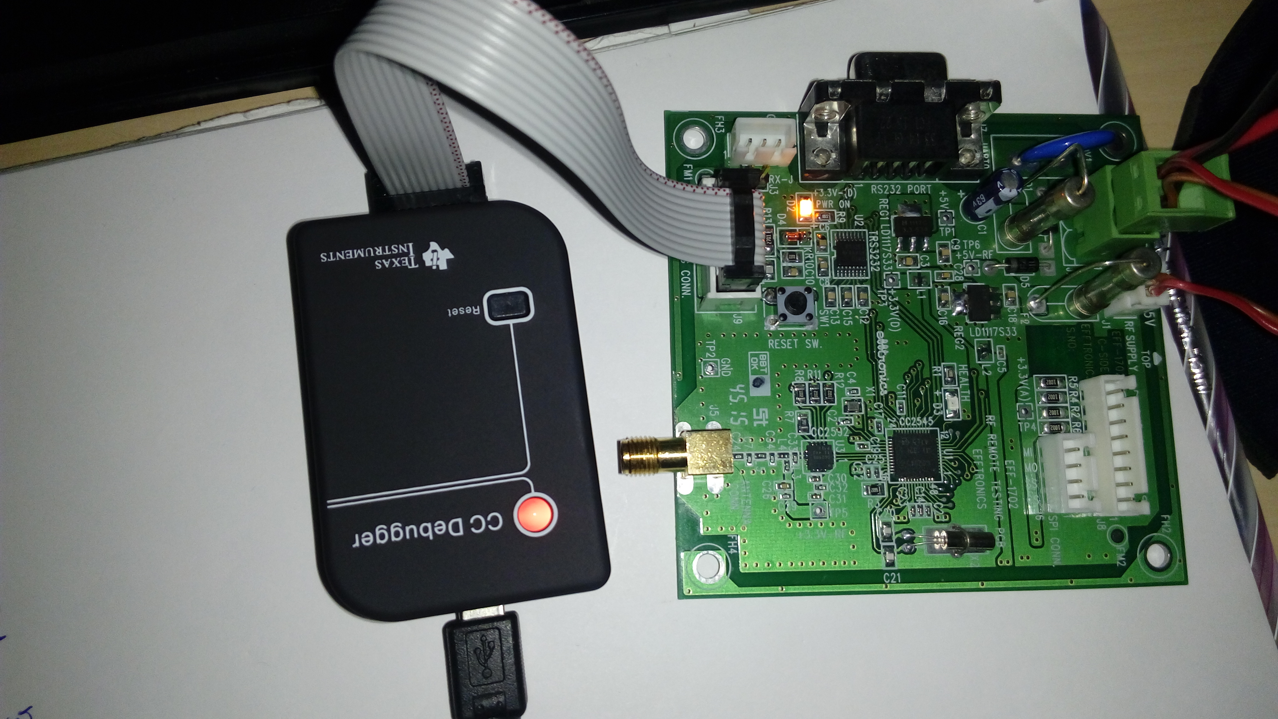
    I disconnect the J9-9 on my board and I confirm the voltage on j9-2 pin as 3V3.Then I was connected to the cc debugger .After this connection we pressed the reset

    Still the led was glowing in red color.

    is there any other bug in the circuit sir?

    regards,

    Manikanta.K
  • Hi,

    In the attached schematics I don't how the cc2545 is connected to ground.

    I do see the cc2592 ground pad is connected to ground through logical pin #17, however,

    I don't see how the cc2545 ground pad is connected to a solid ground.

    When cc254x ground pad is not connected, or not properly soldered to ground, funny things will happen.

  • Manikanta, I tested on my side and CC Debugger detects CC2545 (I have CC debugger firmware revision 0044).
  • Hi Sir,

    Could you please share the connections or hardware setup

    I will compare with your connection sir.

    Regards,

    Manikanta.k

  • Hi Sir,
    Grnd is same through out the circuit sir.

    Regards,
    Manikanta.k
  • Manikanta,
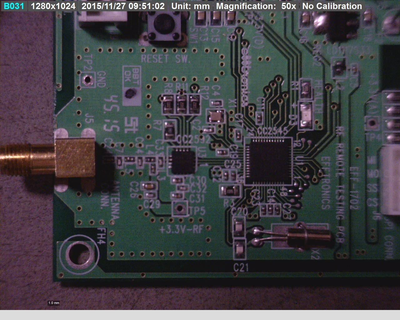
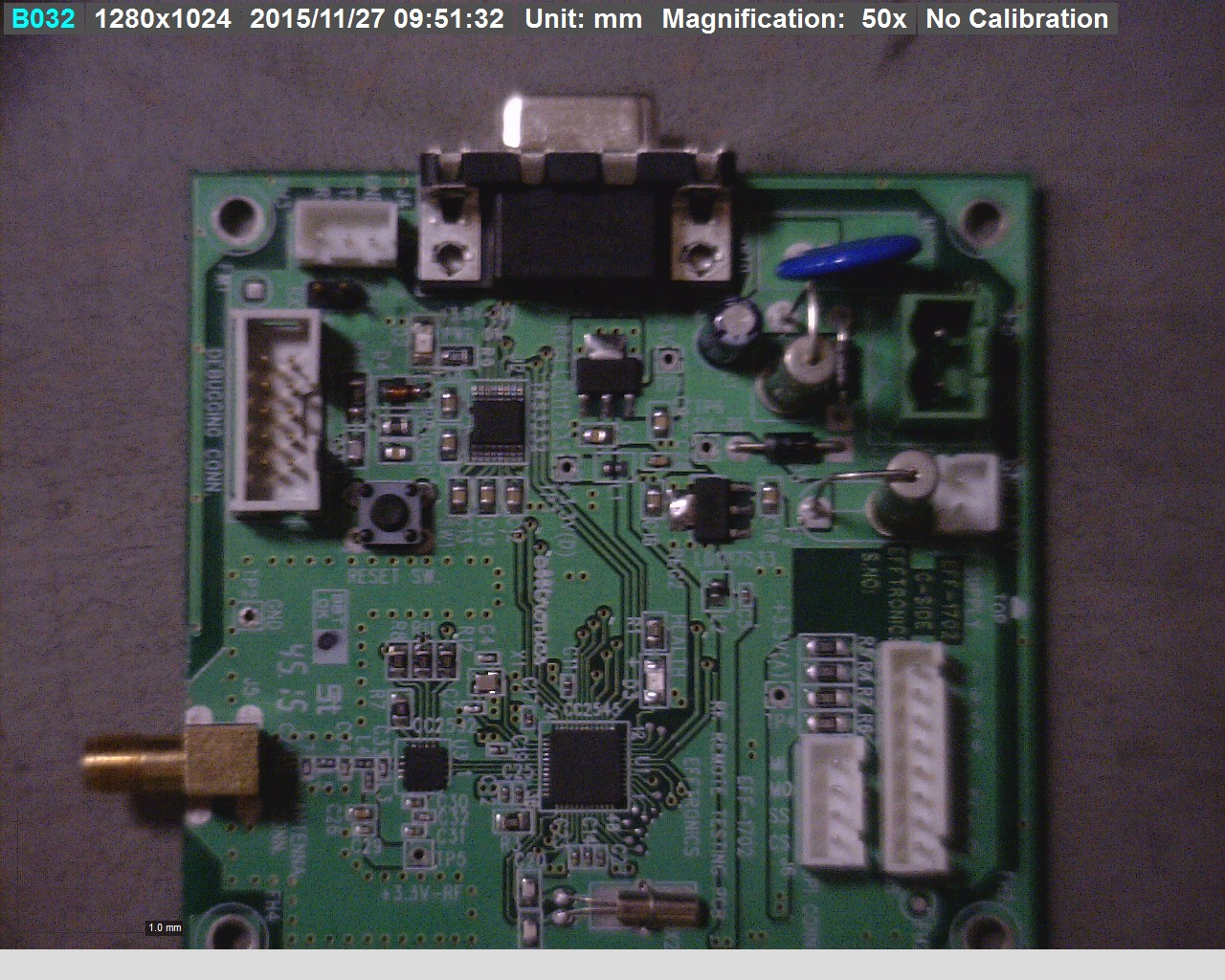
    I connected my CC Debugger to a CC2545EM (mounted on a SOC-BB board). You can see the signal connection by selecting SOC-BB and CC2545EM from this online tool:www.ti.com/.../cross-connect

    From Cross-Connect you can also download the schematics for the 2545EM and SOC-BB board.
  • Hi sir ,

    I was connected the 32Mhz oscillator to the default pins(26 and 27) of the cc2545 chip. After power on the board I kept the probes to the first pin of crystal and to the ground no wave form was generating sir.

    In the part of troubleshooting I removed the crystal in my board and replace in the other board (cc2538 board) .the wave was generated that mean crystal was in working condition.

    could you please verify the schematic which was attached in the above post .where was the problem?

    or else is there any steps needed to do before or after power on the board.

    Regards,

    Manikanta.K
  • Hi Manikanta,

    The crystal is started by SW, so it will not start on an unprogrammed chip.

    Can you check the following voltages: All VDD pins, DCOUPL, Rbias, Reset. Can you also post a photo of the CC2545 section of your board?

    Cheers,
    Fredrik
  • hi sir,

    I was checked the voltage across VDD,DCOUPL,RESET,RBIAS, are as follows:

    VDD:3.3V

    DCOUPL:1.86V

    RBIAS:1.254V

    RESET:3.3V

    CC2545 section as follows:

    Overall board:

    Could you please share the process how the clock will activate through software.

    Regards,

    Manikanta.K

  • Hi Manikanta,

    The boards look good. I really cannot point out any potential problems here. Are you absolutely sure the debug signals are connected correctly? Your debug cable is not too long? Have you looked at the debug signals, including reset, (close to the CC2545) with an oscilloscope?

    How to switch to the 32 MHz crystal oscillator is described in the CC2543/44/45 User Guide. It is typically also the first thing that is done in our SW examples.

    Cheers,
    Fredrik

  • hi sir,

    I am sure that debug signals are connected properly sir.

    After power on I was connected CC debugger as shown in the attached pic.

    We observe the Debug signals and Reset signal in oscilloscope.(All are 3.3V)

    we are not getting clock from crystal after power on the module. By this reason(clock from 32Mhz crystal) CC debugger may be  not detecting the chip.

    As you said SW will generate clock in the before post.

    How we can load the SW into the chip with out detection of CC debugger?

    IS there any other possible way to load the SW ?.

    Regards,

    Manikanta.K

  • When I said measure with oscilloscope the idea was to look at the waveforms while you connect (or reset) the CCDebugger, not at the static voltage after some time. You need to check that the signals on the actual DC, DD and RST pins are as expected.

    The crystal oscillator is started from SW, so as long as you have not programmed the chip this will not start. During programming the chip runs off the internal 16 MHz oscillator. In other words it is expected and correct operation that the crystal does not start up in your case.
  • hi sir,

    The first thing was no clock was oscillating at 26 and 27 pins of the chip.

    As you said internal clock will handle the chip, how we can simulate that 16mhz clock?

    how we can load the SW with out detection of CC debugger?


  • The clock is not your problem!
    - You will not see oscillations on the crystal pins - this is expected
    - The internal clock will start automatically. If all power and ground connections are good, and the chip is not held in reset, no action is required to start this.

    Did you read my previous post? This is what you need to do:
    "When I said measure with oscilloscope the idea was to look at the waveforms while you connect (or reset) the CCDebugger, not at the static voltage after some time. You need to check that the signals on the actual DC, DD and RST pins are as expected. "

    And just to be sure, you are pressing the reset button on the debugger, right?
  • hi sir,

    When am pressing the reset button on the cc debugger ,I could see voltage on the reset pin not completely falling to 0V level.

    But when I press the reset button on my board there is voltage transition from 3.3v to 0v. Connections are verified from my board to cc debugger . If there is issue that chip is not going into reset by pressing the cc debugger(because of no complete transition from 3.3v to 0v) then the chip should go into reset when I press the reset on my pcb.

  • I think I know what your problem is. Remove R10 (and possibly also C10 and D4) and I bet it will work.

    Let me know how it goes and I will explain more.
  • And don't forget to remove C35. :-)
  • No. C35 and R13 are part of the reference design and can be kept in.

    R13 is actually part of the problem, but the solution is not to remove that component. Can you explain why?
  • The reference design says 1nF, not 100nF -> way too much.
  • Hi Sir,

    I was removed the R13 and short with a wire .

    Now I connected the cc debugger it was detected the chip.

    Up to now we got a issue on RESET signal.

  • He has already confirmed that he uses 1 nF (100 nF was a typo). Otherwise you would be correct:)

  • Oh, missed that one, sorry.
  • I said that you should remove R10, not R13. The result will be the same, however R13 is used for filtering and should be kept in the design.

    The reason it does not work is because R10 is almost the same value as R13. Thus when the Debugger tries to reset the chip, it will only be able to pull the reset pin to VDD/2 which is not low enough to trigger a reset.

    The reset pin has an internal 20k pull-up so no external pull is required and R13 should be removed.
  • hi sir,

    if I remove r10 ,the 3.3v and ground will be short when I press the reset button on my board sir.

  • "Remove" is not the same as replacing the resistor with a jumper. You should simply take the resistor away and not put anything in its place.
  • hi sir,

    I was connecting the two cc debuggers at the same time and to the same pc.

    having same usb device id (0000) to the both debugger.

    I am able to open the device control panel on one smart rf studio tool only .

    I am not able to open device control panel on another smart rf studio tool.

    the following window appears :

    Is there any procedure to change the usb device id for the cc debugger.

    or else how to connect the two boards to smart rf studio tool (one as tx and other as RX) at the same time to check the per test?

    Regards,

    Manikanta.K

  • Using 2 CC Debuggers with the same serial number will not work. You must change the device ID on one of them.

    TIABO

  • Hi sir,

    I  interfaced the cc2592(power extender) to the I/O pins of cc2545 chip as following:


    PA_EN -> P0_1

    LNA_EN--> P0_0

    HGM--->P2_0


    I  connected the 2 boards to the PC with 2 cc debuggers to do the per test in smart rf studio tool.

    The device Id's of cc debuggers as follows are 0000 and 8450

    Initially I kept 0000 as TX and 8450 as RX .In this case communication was achieved

    In vice versa case also communication was achieved.

    My query was there is no option for selecting the range extender in Device control panel in smart rf studio tool.

    But cc2592 was mounted on my 2 boards.

    Could you please explain  how data transfer and reception is working without control of cc2592 chip which is in between CC2545 and Antenna.?


    K.manikanta

  • It works because your boards will still radiated, and be able to pick up, some power. This is enough to maintain communication over very short range.

  • hi sir,

    I need to keep one board as transmitter other as receiver permanently.

    for this I done as follows as:

    for receiver:

    1) I kept the LNA_EN and HGM PIN in PA(CC2592) as high by connecting them to 3.3V. and PA _EN as low by connecting to GND.

    for Transmitter:


    1)I kept the PA_EN as high by connecting to the 3.3V and LNA_EN and HGM PIN as low by connecting to GND.

    In this configurations Communication was not achieving.

    Note: I done this connections in hardware.


  • hi sir,

    Previously I said I interface the cc2592(power extender) to the gpio pins of cc2545 chip as following pins:

    PA_EN    ->p0_1

    LNA_EN ->p0_0

    HGM ->p2_0

    As I read Radio test output signals chapter in user manuals.

    By using the OBSSELx registers (OBSSEL0-OBSSEL5) the user can output different signals from the RF

    Core to GPIO pins. These signals can be useful for debugging of low level protocols or control of external

    PA, LNA or switches. The control registers OBSSEL0-OBSSEL5 can be used to override the standard

    GPIO behavior and output RF Core signals (rfc_obs_sig0, rfc_obs_sig1, and rfc_obs_sig2) on pins P1[5:0]

    or P3[5:0]. For a list of available signals, see the description of RFC_OBS_CTRL0 register.


    Could you please give brief explanation about these signals and RFC_OBS_CTRL0 register .

    Is this mandatory to interface the cc2592 to the pins P1[5:0]

    or P3[5:0]? or we can give to any gpio pins as I mentioned above of this post

    if it is able to give any gpio pins. which values have to be placed in RFC_obs_ctrl registers?


  • If the documentation states that those are the only pins that can be used, that is actually the case. There is no way to change that.

    Unless you are making a very simple transmit and receive without ack you must use the RF observation signals to control your PA/LNA.

  • hi sir,

    There is no application note for interfacing the cc2592 to cc2545 chip.

    I was given to the 3 gpio pins as said in the previous post.

    I can't get you in the previous post. Could you please provide the solution for the following query:

    1.can we connect the control signals of CC2592 power extender to the any 3 GPIO pins of CC2545. or not?

    2.Please give the brief explanation about the RF observation signals sir?

  • 1. No, you have to use pins that can be controlled by the RF Observation signals.
    2. Refer to the User's Guide.
  • Hi sir,

    I interfaced to different pins.

    Is there any solution to control the cc2592? without using rf observation signals.

    or else I have to design a new board?

    I was attached my design and board pics and cc2545 section in previous posts in this forum sir.

    Please verify that documents and provide the solution sir.

    Previously I was discussed in CC2545 AHDSP forum

    please verify the following link:

    https://e2e.ti.com/support/wireless_connectivity/f/964/t/450514#pi239031349=5

  • Like Fredrik says, if you have a very simple transmit and receive without ack (which match what you have stated earlier), you can use regular IO pins and set them high and low manually. It is however easier to use the RF observation signals to control your PA/LNA, and these are set to specific pins, that is why we kept refering you to the user guide.
  • Hi sir,

    I was confused with this CC2592 interface.

    Can I use GPIO pins for just transmit and receive tasks or not?

    Please give confirmation sir.

    Or else I will modify and give it to the RF observation signals sir.

  • If you just are using static TX and RX operation then yes, you can use regular GPIO control for the CC2592.

    If you however require acknowledgement of the RF packets then you must use  RF observation signals.

  • thank you sir  for your earlier reply.

    Could you please give clarify on radio configurations in TX and RX.

    IS there any document related radio configuration in TX and RX modes please share the document sir.

    or else please share the steps have to be take in the TX and RX radio configurations.