This thread has been locked.

If you have a related question, please click the "Ask a related question" button in the top right corner. The newly created question will be automatically linked to this question.

CC1101 reference design communication distance

Other Parts Discussed in Thread: CC1101

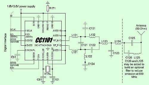
Hi, I am currently working on a project using CC1101 (working at 915MHz range) to transfer data between two boards. I simply copied the reference design from CC1101 document with the 699MHz notch filter. I am using a SMD 868-960MHz antenna from Wurth Elecktronik (part number: 7488910092).

I am able to transfer data between two boards; however, the communication distance is really short. A 0dB transmission output power setting on the transmitter side could only gave me a communication distance of about 15cm, and +11dB output power could get me about 30cm. Any distance greater than 30cm will make them lost communication. 

I used SmartRF along with CC1110 usb dongle to test the radio. It showed that the maximum signal strength (RSSI) I can get is about -70dBm (0dB output) and -50dBm (+11dB output). I also compared it with the TI Chronos Watch that easily gave me about -40dBm for 0dB output power.

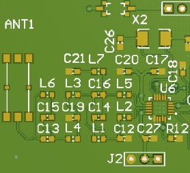
Is there any key point I am missing in my design, like the layout of the circuit? Here is my design: U6 is CC1101, ANT1 is the antenna, and rest are the components from the reference design in between.

Thank you very much in advance!


Yang

  • Hello Yang,

    The layout doesnt looks to be following the reference design Layout, some differences I can see from the picture are that the balun is not symmetrical and does not follow the reference design layout, component orientation is not the same as in TI reference design. These changes can cause mismatch and loss of power transfer resulting in reduced range from the design.

    I will recommend you to exactly copy the reference design for desired performance - board stacking, board dielectric properties (listed in readme file with the reference design), length and width of traces in the RF path and component orientation, use 0402 components, follow the decoupling strucure pin<>capacitor<>via to power.  Have plenty of vias as in the reference design in the RF section.

    Also, when using chip antenna - refer to the chip antenna data sheet for layout recommendation.

    Regards,

    Suyash Jain