Other Parts Discussed in Thread: TRF7970A,
Hello all,
I am facing some problems with the initialization of the TRF7970A as well as reading and writing to the registers.
I am using the TRF7970 Booster Pack (Part No: DLP-7970ABP) with a Nordic controller (nRF5340DK). After having configured all SPI pins (clock, slave select, MOSI and MISO), I am trying to communicate with the TRF7970A device but somehow I cannot receive any information.
I will try to describe all the steps I followed:
First of all, I have initialized the TRF7970A as described in Section 6.11 of the Data Sheet:
- Raise SS and EN after 4 ms. I did not raise EN2, as this is not done in the Reader/Writer application provided by TI (which I successfully tested on my TI Launchpad).
- Issue a Software Initialization Direct Command (0x03 -> SPI MOSI: 0x83), followed by an Idle direct command (0x00 -> SPI MOSI: 0x80)
- 1 ms delay
- Issue a Reset FIFO direct command (0x0F -> SPI MOSI: 0x8F)
- Write the Modulator and SYS_CLK Control register (0x09) with the apropriate application specific setting for the crystal and system clock settings. I wrote 0x01 to the register but I do not really know what should I write here.
- Write the regulator and I/O control register (0x0B) with the appropriate application-specific setting. I wrote 0x00 to the register but I am not sure about that one either.
- Write NFC Target Detection Level register (0x18) with value 0x00. MOSI SPI: 0x18 0x00
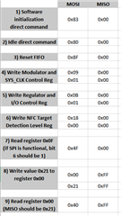
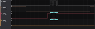
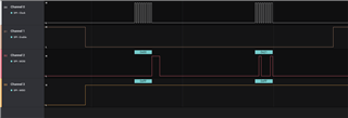
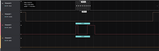
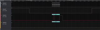
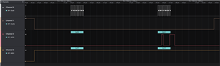
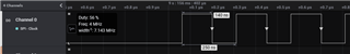
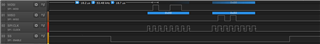
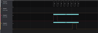
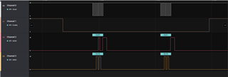
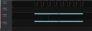
I have used a Logic Analyzer to view the SPI information and I have summarized my results in the following table
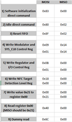
As you can see in the table, the TRF7970A receives information over SPI-MOSI (initialization and some read/write commands) but the data that sends back over SPI-MISO does not really look correct. I can confirm that the "random" values like 0x02 and 0x14 sent over SPI-MISO come from the TRF7970A, as I do not receive them when I remove the TRF7970A from the SPI-pins of my controller.
Being this said, I have a few question about the SPI communication:
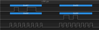
- What does the value 0x02 mean after the Idle direct command and the FIFO reset?
- What does the value 0x14 mean when I write to the Modulator and SYS_CLK Control Register?
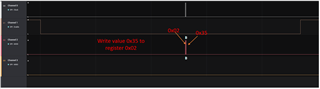
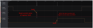
- In step 7 I write 0x21 to the register 0x00. In step 8 I read that register but the information I receive is 0x00. Why cannot I read the value I just wrote?
- In step 9 i perform a dummy read. Why is here as well the received information 0x00?
- Could this be an issue related to steps 5 and 6 of the initialization, where I did not know which values to write to the register?
Looking forward to your feedback.
Many thanks in advance!