This thread has been locked.

If you have a related question, please click the "Ask a related question" button in the top right corner. The newly created question will be automatically linked to this question.

RF430FRL152H: NFC not working

Part Number: RF430FRL152H

Hello Guys,

Good day.

Our customer is developing a little wearable device with our RF430FRL152H. Unfortunately the NFC-connection is not working. They tried the source code on the RF430FRL152HEVM with success, but it is not working on their device. Therefor the problem should be in the hardware. Here is, what they did during the design process:

They designed the spiral antenna with the following dimensions:
N=5; %number of turns
R=12.8 mm; %Outer radius of the outer trace
w=0.5 mm; %Width of the traces
t=0.035 mm; %Height of the trace (or thickness of the copper foil)

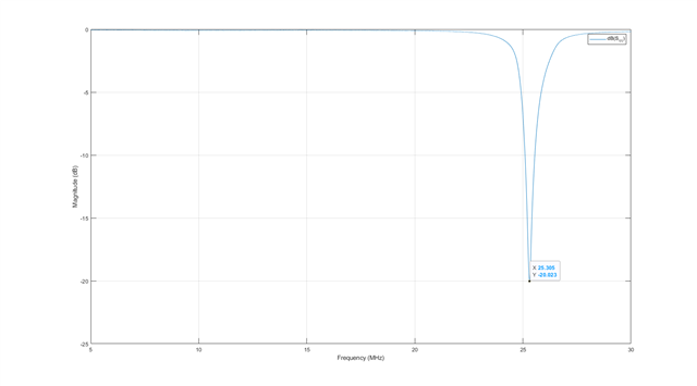
In order to optimize the oscillating circuit, they did an S11-measurement with a network analyzer and a single turn loop antenna. For this measurement there was no external capacitor in the circuit. So only the inductivity of the antenna and the internal capacity of 35pF. The results were as expected:
- the resonant frequency is higher due to parasitic capacities of the board
- in order to reach the optimium natural frequency of 13,7 Mhz, we added capacitors with 84,4 pF

Any advice on why the NFC connection is not working as it does on the RF430FRL152HEVM?

Best regards,

Art

  • Hello Art,

    the reported design seems to be reasonable dimensioned.
    The customer could verify the correct resonance frequency of 13.7 MHz after the 84.4 pF capacitor was added.
    Also the VDDH could be measured at the RF powered application.
    (VDDH is the rectified antenna voltage and can give an indication if the RF430FRL152H got enough power from antenna. VDDH should be >1.8V)
    Also the Q factor of the antenna resonant circuit should be considered.
    More details and practical examples can be found in the following application note: https://www.ti.com/lit/pdf/sloa217

    Best regards,
    Andreas.

  • Hi,

    I haven’t heard back from you for a while, so this tread is being closed. If you wish to continue the discussion, please post a reply with an update below (or create a new thread).

    Best Regards,
    Andreas.

  • Hi Andreas, 

    Good day. Same customer have additional inquiries. I have shared the full details of inquires and it is shown below.

    This is same concern with developing a little wearable device with RF430FRL152H. We want to measure the quality factor of our NFC-circuit as in the SLOA217A - chapter 7.2 decribed. We did this measurement with an network analyzer and a self made single turn loop in Q11-mode. The single turn loop was directly connected to port 1 of the VNA and our device with the RF430FRL152H was coupled per NFC. This are the measurement results: 

    Can we calculate the quality factor with this measurement methode? Or is there anything we should take account at? I ask because of this unknown impedance of the loop probe, which is not calibrated.

    Thank you for your support. 

    Best regards,

    Jonathan

  • Hello Jonathan,

    literature (for example ISBN: 978-0470695067) is describing also this VNA measurement method with coupling coil. So it is a valid method. The real part of the impedance curve should be plotted (rather than S11). The resonant frequency of the measurement coil should be significantly (>2 times) higher than the resonant frequency of the NFC circuit. Also some spacer (ca. 5...10cm) between the antennas would be advisable. If I understood correctly, a calibration measurement of the measurement coil is not required, as long as you plot the real part of the impedance. Alternatively a calibration measurement would allow to directly plot and calculate with the magnitude of the impedance.

    Best regards,

    Andreas.

  • Hi Andreas,

    Apologies for the late update. Here is the customer's response as shown below 


    Thank you for the good literature advice. Just for making it really clear to the costumer:

    In order to compensate the influence, they just have to make sure, that their coupling loop has no significant impact to the measurement in the interesting range (around 10-20 MHz). Than with the measurement of the real part of the coupling loop and the tag magnetally coupled to it, they will get the resonant frequency and quality factor of their tag.

    As it says "the measured transponder impedance is proportional to voltage u2 or current i2" (p.104), wouldn't their measurement in Q11-mode already be fine?

    Best regards,

    Jonathan

  • Hello Jonathan,

    as said before, the coupling loop resonance frequency should be significant higher as the interested range, to avoid overlapping resonant curves. Some distance is required to not disturb the NFC antenna field.

    But I'm not sure if S11 can be used for Q calculation.

    Typically the Q factor is not that critical for new PCB antenna designs, because with the given PCB material and the typical dimensions the Q factor is usually in a reasonable range. Only copper wire antennas may have too high Q factor which, can be corrected with an additional resistor.

    Best regards,

    Andreas.

  • Hi Andreas,

    Our customer wanted to thank you for this great support! This was really helpful for them. They got good results in measurements and they could determine the quality factor also with the S11 measurement.

    Best regards,

    Jonathan

  • Hi Jonathan,

    thanks for the feedback.

    I will close this thread now.

    Thanks and best regards,

    Andreas.