This thread has been locked.

If you have a related question, please click the "Ask a related question" button in the top right corner. The newly created question will be automatically linked to this question.

TRF7960A: tSU,SO definition

Part Number: TRF7960A
Other Parts Discussed in Thread: TRF7970A, TRF7960

Hi Team,


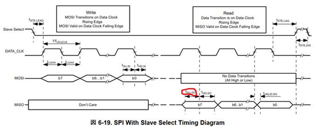
The data sheet of TRF7960A states that Tsu,so goes from the MISO change to the DCLK rise, as shown below. Is this a misleading falling edge? The first bit is also very short.

The data sheet for the TRF7970A was specified with a falling edge.


< The data sheet of TRF7960A : SLOS732G >


< The data sheet of TRF7970A : SLOS743M >


Thanks and Best regards,

 Kuerbis

  • Hi Kuerbis,

    the SPI handling is different between the TRF7960 and TRF7970. Please see the following documents:

    FAQ chapter 4.1  https://www.ti.com/lit/sloa248

    and https://www.ti.com/lit/sloa140

    Best Regards,

    Helfried

  • Hi Helfried,

    Thank you for replying.

    OK. You men that the tSU,SO timing in the data sheet of TRF7960A : SLOS732G is correct. Right?

    It seems B7 bit is very short at Figure 6-17. SPI With Slave Select Timing in The data sheet of TRF7960A : SLOS732G as above. Their is no one data clock.

    Let me confirm that it's actually one data clock cycle in https://www.ti.com/lit/sloa140 which you mentioned as below?

    Thanks and Best regards,

     Kuerbis

    .

  • Hi Kuerbis,

    after checking figure 6-17 of the TRF7960A datasheet in detail, I see this diagram is incorrect. It states also wrong MOSI instead of MISO in the description of the Read Mode.

    Please stay with the document sloa140 which is correct.

    Data output on the MISO line will go active in read mode at the rising clock edge and the data will be take at the falling clock edge.

    Best Regards,

    Helfried

  • Hi Helfried,

    How is the definition of tSU,SO?  

    I would like to confirm the following parameter timing definition like in the datasheet.  There is no such a information in sloa140.   Which edge is the specification for?

    tSU,SO MISO input data setup time
    tHD,SO MISO input data hold time
    tVALID,SO MISO output data valid

    Thanks and Best regards,

      Kuerbis

  • Hi Kuerbis,

    lets's see if we come closeer when thinking about the general function. The master wants to read data from the slave. The master sends the clocks to the slave and the slave changes the output data at the rising edge of the clock which needs the time specified as tVALID,SO. Then at the falling edge the slave has to do nothing but the master has to validate the data at the MISO line.

    When using the recommended 2MHz clock the slave will send valid data on the MISO line after max. 75ns, the next falling edge occurs after 250ns, so the master has a setup time of 175ns. The next rising edge occurs after 250ns. The slave will then change the MISO line again. This give the master a hold time of 250ns + tVALID,SO which is min. 250ns + 30ns = 280ns.

    From my standpoint it makes no sense to specify a setup or hold time for the MISO line from the slave side. This is a spec for the master not for the slave.

    Can you please explain why this parameter would be essential for you.

     Best Regards,

    Helfried

  • Hi Helfried,

    I understand this spec is for the master.  So the customer needs the edge for tSU,SO MISO and tHD,SO.

    I would like confirm the MISO behavior vs. SCLK.

    I'm confused that In case of CKPH-0, CLPL-0, MSP430 require SPI timing in the data sheet of TRF7960A : SLOS732G.  Right?

    Thanks and Best regards,

     Kuerbis

  • Hi Kuerbis,

    the timing diagram for the TRF79xx SPI read specifies a setup and hold time which makes no sense for an output. The only relevant timing parameter in this case is the tVALID time which defines the delay from the rising clock edge until the SOMI line is stable. The MCU (Master) will validate the data on the SOMI line with the falling edge of the clock. The max clock speed depends on the output delay of the TRF and the setup and hold time requirements of the MCU.

    The specification of  tSU,SO and tHD,SO  for the SPI read should be removed from the TRF datasheet.

    Best Regards,

    Helfried

  • HI Helfried,


    Thank you for providing the summary. I understand it.


    Thanks and Best regards,

     Kuerbis