This thread has been locked.

If you have a related question, please click the "Ask a related question" button in the top right corner. The newly created question will be automatically linked to this question.

RF430FRL152H: trying to program rf430frl152h

Part Number: RF430FRL152H
Other Parts Discussed in Thread: MSP-FET,

Hi Experts,

Our customer is trying to program the RF430FRL152H chip by its EVM JTAG schematic but wonders if the power3V3 is needed
He came across a question in the forum saying that is unnecessary
e2e.ti.com/.../level-shifter-for-jtag-from-fet-to-rf430frl152-with-sn74lvc2g125-and-sn74auc1g04

He is asking what is he supposed to do if it is unnecessary? like connect it to the ground or just connect nothing?

and another question is if these so-called necessary caps and resistors are needed when programming.
what the customer focuses on is the JTAG module and especially for the POWER_3V3. He thought there are 3 possibilities: perceive it as MSP_VCC and connect it to JTAG pin2/connect it to nothing(then 2 relevant resistors R32 and R34 can be removed as well)/connect it to GND. and then it doesn't give the answer if the necessary caps and resistors are needed when programming the chip. He said: "i must declare that all i am intending to do now is to burn the chip successfully"

The customer also said "the power_3v3 is sure to be unnecessary for programming since it comes from the USB power supply(you can confirm this from the power section schematics in the user guide), and we don't need to connect the EVM to the USB while programming the EVM by MSP-FET(also be confirmed in the user guide ). What I need to know is how should I handle this to ensure that I can burn the chip successfully"

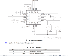
And to make sure the customer can program the chip he also need to know if the external components are required when programming(see in RF430FRL15xH FAQ file 2.3)

e2e.ti.com/.../rf430frl152h-troubles-connecting-programming-via-jtag
it seems that this guy has added the external components to burn the chip

We hope to hear your advice. Thank you so much in advance.

Kind regards,

Gerald

  • Hi Gerald,

    This thread will be addressed in the next few days once a specific expert has come back from vacation. Thanks for your patience in the meantime. 

  • Hello Gerald,

    sorry for the delayed response. I just returned from vacation.

    I only can comment to the original RF430FRL152HEVM schematics, as the provided screenshot does not show any level shifters.

    For the use case of programming and debugging the RF430FRL152HEVM with an MSP-FET the POWER_3V3 supply is not required, as the MSP-FET is providing the FET_VCC. I guess the voltage at POWER_3V3 is 0V in this case, but it doesn't matter due to diode D3 is blocking a reverse current. If the customer use case is not requiring USB supply, then it would be possible to remove the POWER_3V3 related components. If connecting a booster pack is also not required, then the RF430_RST path (R32, R34) can also be removed.

    The required external components, shown in section 2.3 of the FAQ document are necessary for the typical application use case. If the ultimate goal is only the programming via MSP-FET and no applicative operation, then L1, C1 and all components at pins 11...18 are not required. B1 would be replaced by POWER_1V5 of the IC1 of the EVM. And it would be necessary to connect VDDB to VDDSW, as it is done with the jumper SV7 at the EVM.

    To summarize, the following components on the RF430FRL152HEVM are essential for programming via MSP-FET:

    SV7 (closed), C13, C12, C17...C19, C24, IC4...IC6, IC8, R19, R22...R26, R28...R30, SV2, IC1, C9, D3, C3, S6 (in position "Supply"), R5, C11.

    Let me know if you have further questions.

    Best regards,

    Andreas.

  • Hi,

    There was no feedback since a while, so I assume this tread is resolved and can be closed. You can still reply to this thread after it is closed, or you can create a new thread.

    Best  Regards,
    Andreas.