This thread has been locked.

If you have a related question, please click the "Ask a related question" button in the top right corner. The newly created question will be automatically linked to this question.

I want to know the output impedence and input impedence of CC2530

Other Parts Discussed in Thread: CC2530, CC2591, CC2520, CC2500

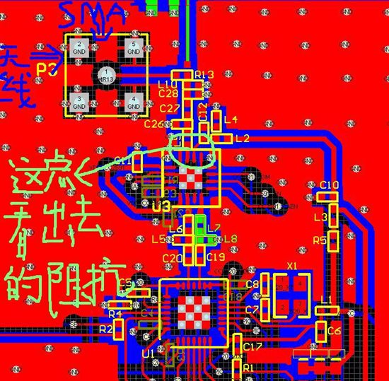
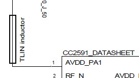
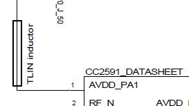
        I want to know the output impedence and input impedence of  CC2530. I also want to know the output impedence and input impedence of  CC2520.I have looked for many  resource.But I can not find the value.who can tell me?

      Thanks.

     Respectfully,

     stones yang 

  • Stones,

    The spec load impedance for the CC2530 is 69+j29.  We don't provide an output impedance.    You match to this value by taking the conjugate and design the matching network. 

    Regards,

  • RSS,

            Can you tell me the output impedance of CC2520?  At the same time I also want to know the output impedance of CC2591.Please tell me.

            Thanks in advance.

            Regards,

           stones.

  • Stone,

    The TI radios don't list an output impedance becasue you have an LNA and Power Amp which you need to match.  We tune this to be very close then provide you based upon load pull measurements the best impedance to match for stabillity and power transfer.    I gave you that value it now is a matter of doing a conjugate match.  AN068 which covers this with an example of the CC2500 which has the same output impedance load requirement.    The output impedance of the CC2591 best load match is at 33+j7.  At the same time you probably like to change it impedance to 50+j0 to match an antenna.    There are many electronic version of Smith Charts which allow you to come up with these values.   In addition their are web-sites which calculate based upon the vector values.    One I use occasionally is http://home.sandiego.edu/~ekim/e194rfs01/jwmatcher/matcher2.html,   Keep in mind this site does not include the PCB trace impedances so it will not be as exact as using a simulator 3-D tool like ADS from Agilent.   This takes into account the trace impedance and the fields to give an exact match.    We find it to be accurate to the component tolerance. 

    Rgds

  • RSS,

    Thanks for answering my question.Now I have  designed  CC2520+cc2591 board  with 2-layer PCB. But it can not send any signal. So i doubt  if i want to use CC2591,CC2591  must   be  on  4-layer  PCB.Using CC2591  almost  can not  succeed with   2-layer PCB. Is it right?Below is my board that can not send any signal.

    Thanks in advance.

    Regards,

    stones.

  • Stones,

    Not working at all has nothing to do with the matching.    The most common problem with the combo is the cusotmer did not program the CC2591 with correct polarity signals so the CC2591 is in TX mode when the radio is programmed to do a TX  and similarly with RX mod.    Please use an scople and check the polartiy of the control signals to the CC2591.  It sounds like you are not programming correctly.  The polarity of the signals is given in the data sheet.

    A 2-side board will work but your preformance will degrade if you don't keep the impedance of the traces the same as the 4-side board.  TI uses the 4-side board so the second layer thickness is small allowing for smaller traces that are of certain impedances.    Thicker baord the line widths will get larger and take up to much room.

    Rgds


  • RSS

    What is the polarity signal?Sorry,I do not know how to program the polarity signal.I just copy the TI PCB layout.Which data sheet can I find the polarity of signal?

    Thanks in advance.

    Regards,

    stones.

  • Stones,

    The load impedance is a vector with a real and imiganary part.   the Imiganary part can be negative or posiive which relates if it is capacitivie or inductive.   The polarity of the signal is make on the data sheet of the RF pins.  this is not digital but differential analog signals,  which means at any instance in time it could be plus or negative.   If you are having trouble getting the CC2591 programmed why al the questions about the impedance?   It seems your problem is not program the signal so it appears at the output of the CC2591.    if you copied the layout exactly then it should be a problem.   This means with the same layer stacking and trace widths.   If you changed the layout you will degrade the performance but once again if you not getting a signal through CC2591 it probably isn't imedance issues.    Once you see a signal using a spectrum analyer then we can discuss matching impedances.

    Rgds,

  • RSS

    I use 2-layer PCB.Stack of board is 1mm.

    Regards,

    stones.

  • Stones,

    1 mm will change the matching impedance but this probably is not what makes it not work at all.   You probably see a few dB of change in power, so focus upon why the CC2591 is not  working in TX and RX mode.


    Rgds

  • RRS,

    I am sure Program is OK.Because I  make two board.I use the same program,The other board can send signal.But its distance is only 5-6m.

    I use a digital voltmeter to measure the volatge of CC2591 RF pin.The digital voltmeter displays 0-4v.So can i make a conclusion that  CC2591  works  well?

    Thanks in advance.

    Regards,

    stones 

  • RRS,

    Are you online?I am eager for your reply.

    Thanks in advance.

    Regards,

    stones

  • Stone,

    I'm going to give you the trouble shooting methods we use to bring up a new design.   Please follow it and you should be able to isolate your problem.


    1)  Check all power at the IC pins to make sure they are at 3.3V  +/- 0.2

    2)  Make sure all digital lines to the CC2591 are at the correct high or low for the conditions specified in the Data Sheet

    3) Do not use the processor but connect from a SmartRF Studio board  the following wires Data,  Clk,  RST,  3.3V and Gnd

    4) Program the chip for a signal unmodulated carrier at a selected channel frequency.   Program the chip to TX mode

    5) Between the antenna and balun/filter output connect to your SMA

    6) Read the Power into a spectrum analyzer with 50 ohm termination.

    7) If power peak power reads the same as the program entry then the balun/Filter is OK.

    8) Measure the antenna resonance with a VNA, steps are shown in DN001 application note found on TI web site

    9) If impedance is not 50+j0 record and rematch to the output impedance of the Balun/Filter

            Note this assumes you copied the RF balun/filter network exactly like a TI refernece design and didn't change the board thickness or layers,  traces or component vendors

    10)   Using the SmartRF Studio cards program two EM modules from TI with equivalent parts and whip antennas.   Set them about 1 - 3 meters apart.   Put one in TX mode and one in RX mode.    Record the RSSI for the TI boards.    Switch to your design and repeat the steps.   If the RSSI is the same your board is working OK

    11) Complete LOS measurements to validate the system.

    You must use Spectrum Analyzers and Vector Network Analyzers for RF measurements.    When using vector network analyzer you must calibrate to a calibration kit and understand how to de-embed your measurements.    There are plenty of web sites which explain s-paramters.

    12)  Check running your software and if TX and RX change you have incorrectly programmed the two parts.  Review the software in the SmartRF Studio card with your system.

    This should be simple enough to follow and you don't need me to OK each step.   The TI boards are reference layouits which have been tuned for maximum performance.  Use them in your trouble shooting by following the steps above and you should have success in getting your board to work.

    Rgds

  • RRS,

    I have changed the board thickness and layers.I use 2-layer RF4 PCB.What's worse,i do not copy TI reference design exactly.My PCB has been released above.I think you should have seen.Maybe I have better to design again.555~

    Regards,

    stones

  • RRS,

    how can i decide the length of  trace of 50 ohm?It is between SMA and resistance in "CC2591 +CC2520" refernece.Below is the trace.


    And what are the values of these TLIN inductor in "CC2520+CC291"?I do not take these into account.Maybe these elements lead into problem.  

    Regards,

    stones


  • Attached is a microstrip line calculator I download fromt he web.   0083.txline.zip


    Regards,

  • RRS,

             I find impedance of trace has nothing with length of trace.So I don't know how to decide the length of trace.And I want to know the value of TLIN inductor in "cc2520+cc2591".Can you tell me?

    Thanks in advance.

    Regards,

    stones

  • Stones,

    Once again we only give the load impedance which is found on page 7 of the data sheet.     Use the conjugate of this number to calculate your matching network. 

    Rgds

  • Using the line calculator and enter the length width and permittivity found in the text file to get the impedance at  a particular board height.   You can use the same line calculator to calculate the values for a different board height.

    Rgds

  • RRS,

    Thanks for you reply very much.Maybe my english is poor.You did not catch me.I know how to calculate the impedance of line.But I do not know how to calculate the inductor of line that is emphasized in the picture.


    Rgds,

    stones

  • I use the tool you suggest to calculating the impedance matching , I have a question what Q factor i should use during my calculations ?? what is the best , I am using cc2530 2.4 GHz