


Hi friends,
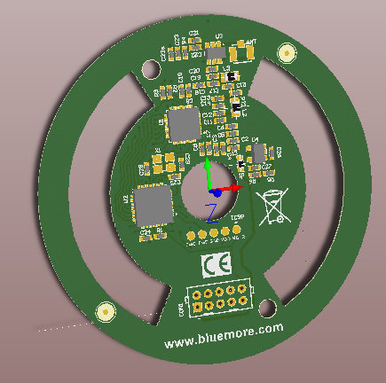
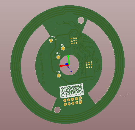
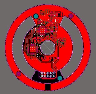
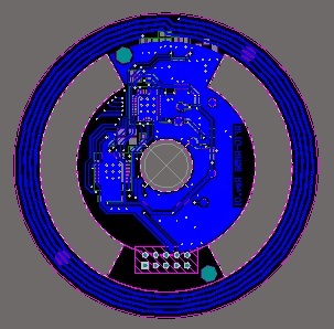
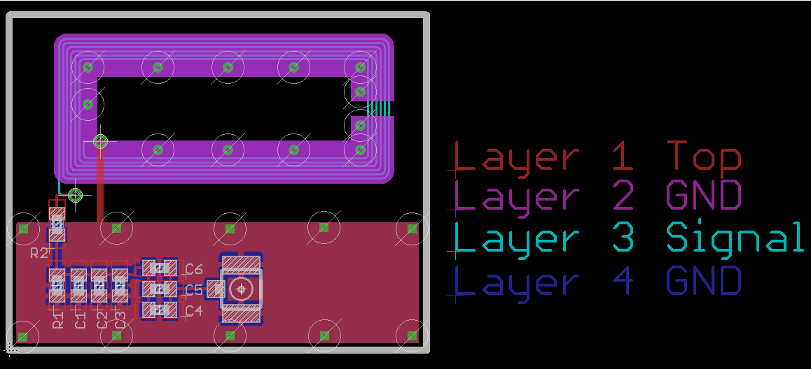
I wokrd before with NXP RFID chips and when design PCB antenna they suggest that for example on top layer I have few turns of PCB track inductance about 1200nH, and on bottom layer GND under that tracks like shield. Now I am looking TRF7970A chip and older TRF7960A and see that they use PCB tracks but on bottom layer no ground plane under track lines, where NXP suggest that. What is your experience. I want to make module with TRF7970 and PCB antenna that will have header connector so plug on my main board above.
Darko


