Part Number: TRF7960A
Other Parts Discussed in Thread: MSPM0L1306, SYSCONFIG
Tool/software:
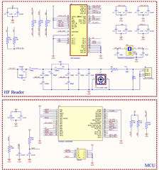
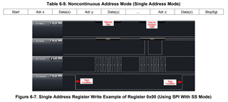
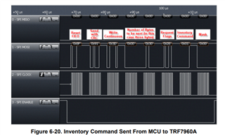
Hello, I made a board based on TRF7960A reader, controlled by a MSPM0L1306 MCU, above, you can see the schematic of such board. For the coding, I want to go step by step, and right now I am trying to read a simple register value. But the response I get is always 0x00 (probably the reading request didn´t even get to the IC). The SPI interface configured through sysconfig tool with no interrupts, 2MHz data rate, Motorola 3-wire (I am handling CS signal independently), the clock polarity and phase are initially 0 (clock polarity goes to 1 when reading mode). I activated CLK, MISO and MOSI internal pull-down resistors so when I disable SPI to change the clock polarity they don´t go to high impedance (I don´t know if that´s what happens). Can you help me to identify and fix the problem (it may be a hardware issue as well)?
#include "mspm0l130x.h"
#include "stdio.h"
#include "ti_msp_dl_config.h"

// Macros
#define HWREG(x) (*((volatile uint32_t *)(x)))

// Registers
#define Status_Control 0x00
#define ISO_Control 0x01
#define Tx_Pulse_Lenght_Ctrl 0x06
#define Rx_No_Resp_Wait_Time 0x07
#define Rx_Wait_Time_Register 0x08
#define Mod_Register 0x09
#define Rx_Special_Settings 0x0A
#define IRQ_Status 0x0C
#define IRQ_Mask 0x0D
#define FIFO_Status 0x1C
#define FIFO_Register 0x1F

// Constants
#define ISO14443A 0x08
#define OOK 0x21
#define Enable_RF 0x21
#define Disable_RF 0x01
#define Pulse_Lenght 0x20
#define No_Resp_Wait_Time 0x0E
#define Rx_Wait_Time 0x07
#define Special_Setting 0x20
#define IRQ_Mask_Set 0x3E
#define REQA_Command 0x26
#define ISO14443A_No_CRC 0x88
#define End_of_Tx_IRQ 0x80
#define End_of_Rx_IRQ 0x40
#define Collision_IRQ 0x02
#define SPI_Phase0 0x00000007
#define SPI_Phase1 0x00000207
#define SPI_Pol1 0x00000107
#define SPI_Pol0 0x00000007

// Direct Commands
#define SW_Init 0x03
#define Rst_FIFO 0x0F

// Function Prototypes
void TRF7960A_Init(void);
void TRF7960A_WriteRegister(uint8_t addr, uint8_t data);
uint8_t TRF7960A_ReadRegister(uint8_t addr);
void TRF7960A_DirectCommand(uint8_t cmd);

// Global variables
uint8_t reg_value = 2;

int main(void)
{
    SYSCFG_DL_init();

    DL_GPIO_setPins(TRF7960A_PINS_PORT, TRF7960A_PINS_SS_PIN); // SS to high

    TRF7960A_Init(); // Configuring TRF7960A

    while (1) {

        reg_value = TRF7960A_ReadRegister(ISO_Control);

        printf("%x\n", reg_value);

        delay_cycles(64000000); // 2s delay
    }

}

// Initializate TRF7960A
void TRF7960A_Init(void) {
    // ISO14443A configuration
    TRF7960A_DirectCommand(SW_Init); // Power Up
        delay_cycles(320000); // 10ms delay to wait for TRF7960A clock stabilization

    TRF7960A_WriteRegister(ISO_Control, ISO14443A); // ISO14443A 106kbps
    TRF7960A_WriteRegister(Mod_Register, OOK); // OOK (100%), 6.78MHz Clock (not used)
}

// Write in TRF7960A registers
void TRF7960A_WriteRegister(uint8_t addr, uint8_t data) {
    uint8_t cmd = (0x00 | addr) & 0x1F; // (0x00 | addr): B6 to Write Mode (0). (& 0x1F): To guarantee B4-B0 right address

    printf("%x\n", cmd);

    DL_GPIO_clearPins(TRF7960A_PINS_PORT, TRF7960A_PINS_SS_PIN); // SS to low
    DL_SPI_transmitDataBlocking8(SPI_0_INST, cmd); // Transmit the address of the desired register to write

    DL_SPI_transmitDataBlocking8(SPI_0_INST, data); // Write the desired value on the register

    DL_GPIO_setPins(TRF7960A_PINS_PORT, TRF7960A_PINS_SS_PIN); // SS to high
}

// Read a TRF7960A register
uint8_t TRF7960A_ReadRegister(uint8_t addr) {
    uint8_t cmd = (0x40 | addr) & 0x5F; // B6 to Read Mode (1). (& 0x5F): To guarantee B4-B0 right address
    uint8_t data = 1;

    printf("%x\n", cmd);

    DL_GPIO_clearPins(TRF7960A_PINS_PORT, TRF7960A_PINS_SS_PIN); // SS to low
    DL_SPI_transmitDataBlocking8(SPI_0_INST, cmd); // Transmit the address of the desired register to read

    DL_SPI_disable(SPI0);
    HWREG(SPI0_BASE + 0x1100) = SPI_Pol1; // SPI clock polarity = 1
    DL_SPI_enable(SPI0);

    data = DL_SPI_receiveDataBlocking8(SPI_0_INST);

    DL_SPI_disable(SPI0);
    HWREG(SPI0_BASE + 0x1100) = SPI_Pol0; // SPI clock polarity = 0
    DL_SPI_enable(SPI0);

    DL_GPIO_setPins(TRF7960A_PINS_PORT, TRF7960A_PINS_SS_PIN); // SS to high

    return data;
}