Other Parts Discussed in Thread: CC2520
Tool/software:
Hi,
In several threads, it has been suggested that the output impedance of the CC2590 is around 33 – j7 Ω. However, after extensive matching experiments using a custom antenna design, I’ve yet to observe any resonance or performance peak near that point — even when tuning directly toward its conjugate.
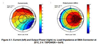
Looking at TI Design Note DN037 (swra375), particularly Figure 4.1 (right side), it seems the maximum output power is achieved at an impedance noticeably more resistive than 50 Ω, assuming the chart is normalized to 50 Ω. This doesn’t align well with the 33 – j7 Ω assumption — unless the chart is normalized differently, which is unclear from the figure. Can anyone confirm what the Smith chart in DN037 is actually referenced to?
Given that I can’t follow the reference design directly (different antenna, board size, layout, and environment), I’d appreciate clarification on the realistic ballpark of the CC2590 output impedance, or any characterization data. Is it in fact closer to 50–60 Ω, or perhaps even higher?
Also, I’m operating the CC2590 at 2.3 V Vdd, not 3.0 V. Could the output impedance shift further toward higher resistance at lower supply voltages due to reduced PA drive capability?
Thanks in advance for any insights — they would be highly valuable for tuning this properly.
BR, Ilkka