CC2651R3SIPA: PCB ;ayout guideline for CC2651rsipa

Part Number: CC2651R3SIPA

Tool/software:

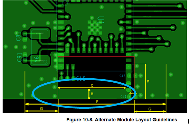
We use the layout guidelines mentioned in the device datasheet. some are reproduced here

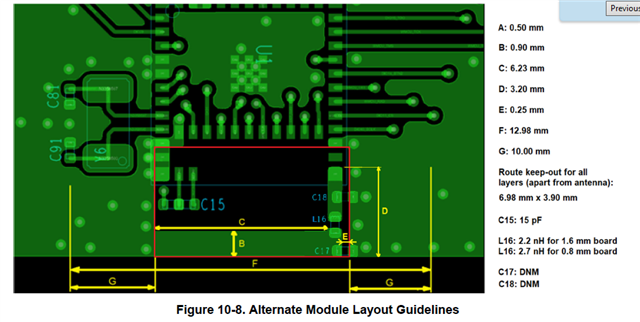
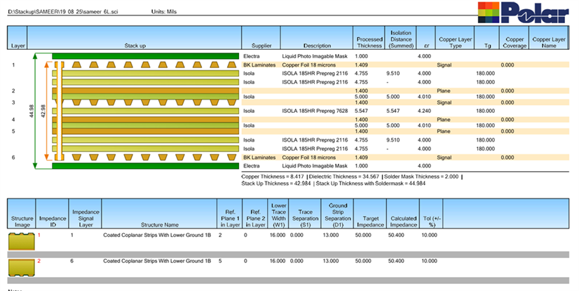
For our layer stackup, the 50 ohm track width is 0.406 mm(16 mils), Whether the above dimension A through

G willm change accordingly, if so what is the values for A through G

thanks

  • Please share your stack-up first. I do not want to assume and give you the wrong feedback.

    Bun

  • the layer stackup planned is given below.

    Please clarify the following in addition to the question raised.

    1. In page no 60 of datasheet it is mentioned that "The ground loop should only be

          on the top layer of the board and not on all 4-layers", whether it means 

        highlighed area in blue color in the following 

          layout needs to be there in the layer where the device is mounted and to

         be removed in all layers, we have six layers, then whether it needs to be removed in all 

         5 layers.

    2. Whether the pi network in antenna ground pin to ground loop needs to follow the track width of 16 mil as mentioned 

        in the attached stackup

    3. Whether green solder mask can be applied on top of Antenna GND pin connection to Ground look

    4. This is the 3rd version HW for using CC2651R3sipa. in the first two versions we

       got 10 dB less received power compared to CC2651R3SIPA launcher kit from TI,

       Why this much less power in our HW, how to reduce the loss.

    Thank you

  • Regarding your initial question, we do not recommend changing the stack-up, but if it is unavoidable, then tuning the antenna match filter can readjust the frequency response.

    1. Will need to double check with greater team

    2. If you referring to Dimension A in figure 10-4, then it is 19.7mils. The idea is to match the dimensions of the ground pad at the top of the PI filter.

    3. No, we generally do not apply soldermask to any pins.

    4. I'm assuming the 3rd version of the your PCB does not have this issue? If so what has changed?

    Bun

  • I request some clarification based on your inputs,

    1. Will need to double check with greater team


    In page no 60 of datasheet it is mentioned that "The ground loop should only be on the top layer of the board and not on all 4-layers", I understood that the  highlighed area in blue color in the following layout needs to be there in the layer where the device is mounted and to  be removed in all layers. But in the device design files from TI swrc382.zip, the ground loop connection for the antenna pin is there in all four layers.

    What I need to do whether to remove in all other layers or hold it.

    2. If you referring to Dimension A in figure 10-4, then it is 19.7mils. The idea is to match the dimensions of the ground pad at the top of the PI filter.

    We try for 4 layers  if possible for our application, if so we follow the stackup & trackwidth recommended in the datasheet,  If we need 6 layer and use the stackup attached above, whether we can follow the recommended track width of 16 mils for 6 layer stackup, if so what other checks/changes we need to do for our PCB layout.

    3. No, we generally do not apply soldermask to any pins.

    Whether we have to remove green solder mask in the tracks and pi network connected to the antenna ground pin for better performance. I came across some references where it is recommended to remove solder mask in RF tracks and antenna feed lines.

    4. I'm assuming the 3rd version of the your PCB does not have this issue? If so what has changed?

    This PCB is the 3rd version of our HW using CC26513RSIPA. In the previous 2 versions it is 6 layer PCB. In the previous 2 versions we observed 10 dB less RSSI compared to similar setup with Launch (PAD)kit for CC26513RSIPA, how we can get similar performance as that of CC26513RSIPA Launch PAD HW from TI.

    I need to proceed for PCB layout. Your inputs are required to proceed.

    Thank you. 

  • 2. In this case, the impedance of the trace does not have much impact as the length is short, but the discontinuity between pad and trace width will have a greater impact on antenna performance. We do not recommend changing the dimensions instead adjust the antenna match circuit.

    3. No need to remove soldermask here as antenna performance has been validated with the soldermask.

    4. I believe you are saying that all 3 version has less power than the LP assuming this is radiated power the most likely cause is the stack-up and antenna dimensions because these parameters can completely shift the impendence of the chip itself and invalidate all filter circuits on the RF path.

    Bun

  • AS per the datasheet, the 50 ohm impedance trackwidth needs to be 0.3 mm - 11.811 mil (table 10.6), but the track width used in the layout snapshot shown in page 57 looks like 0.388 mm - 13.5 mil (as per page no. 75 of datasheet). But the following track for pin 14 and 15 are planned as per what calculation.

    Whether the track width  for connecting the "antenna ground" (pin 16)  pin connection to ground loop is planned to match the pin pad size or how it is decided.

    thanks.

  • Regarding Question #1 about the ground loop, it is the area you have shown, but only applies to the single-layer design (Figure 10-8) hence the comment. Antenna tuning is on the signal-layer is achieved through the matching circuit through. The 4-layer design in Figure 10-4 does not require a matching circuit but the dimension and stack-up must match the reference design.

    As for the track width, this is determined through EM simulations which gives you a better view of all the antenna parameters, such as efficiency, bandwidth, directivity, etc. Matching to 50 ohms is only part of the picture.

    Bun