This thread has been locked.

If you have a related question, please click the "Ask a related question" button in the top right corner. The newly created question will be automatically linked to this question.

Layout connsiderations for chip antenna for 868 MHz

Other Parts Discussed in Thread: CC1150

Hi,

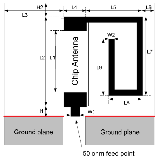
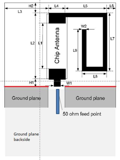
  I am using CC1150 transmitter and a chip antenna from Johanson technolgy. The image shows the reference layout of the antenna. The ground plane shown in the shaded area has to be in the same layer as the pcb trace attached to antenna or is it ok if its on the lower layer? Also if I put it on the same layer is there minimum width of the ground pour required  from the edge(marked red) for it to function properly?

  • To complete the design you will add the transmission line that connects to the point labeled "50 ohm feed point". This line must be a controlled impedance line and therefore must be over a ground plane thus the ground plane would be on the side opposite of the side the antenna pattern is on. It is important that this ground plane be continuous all the way back to, and under the CC1150. It can have several vias and even a short line or two between vias but otherwise it must be a solid field with nothing crossing under the transmission line shown in blue. This line will be narrower than W1 since it is over a ground plane and the antenna is not.

    For 50 ohms the blue transmission line width will be about 1.67 X the board thickness measure from the top layer to the ground plane under the line assuming FR4 (Er 4.3). This is not the total board thickness unless it is a 2 layer board with the line on top and the ground plane on the back. There are numerous free impedance calculators on line. You will need to know the layer 1 to 2 thickness for you particular PCB fab shop.

    On a 4 layer board the ground plane is typically layer 2 to ensure it is a continuous plane under the top layer without signal traces.

    Copper pour on top with multiple vias to the backside ground is recommended. The topside pour to transmission line gap should be at least 3 dielectric thicknesses.

    Dielectric thickness = board thickness between the line and the ground plane.