This thread has been locked.

If you have a related question, please click the "Ask a related question" button in the top right corner. The newly created question will be automatically linked to this question.

Pls help me to check the Inverted-F Antenna Design

Other Parts Discussed in Thread: CC2530, CC2591

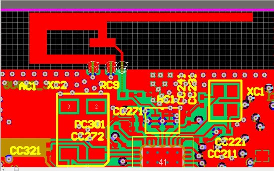
Hi, I am working on a customized PCB design for CC2530 with balun 2450BM15A0002E from Johanson Technology and the Inverted-F Antenna from DN0007. Here is a screenshot of my design. Can anyone of you please help me to see if there is anything wrong/bad with my design for the Inverted-F Antenna, especially to clear my doubt for microstrip?

Here I use an L-match network (with a paralleled capacitor and a cascaded resistor) between the balun and the antenna. The width of the microstrips is 0.182mm (7.165mil) for a 50 ohm impedance. I made it this width because I use a 6-layer FR4 board, the distance between top layer and ground plane (the 1st inner-layer with the shortest distance from top layer) is 0.123mm. But the pads of the cascaded resistor is much larger than the microstrips, will it be a problem for the antenna??

If I change the ground plane to the next layer (the 2nd inner-layer which has a distance of 0.553mm from top layer), the width of microstrip lines will be 1.024mm (40.35mil). In this case the width of microstrip lines is much wider than the feed point of antanne (10 mil), will I get a high return loss at the connecting point with the antenna?

I am wondering which choice for the width of microstrips will be much better, to get a better performance?

I hope anyone who has a clearer idea would give me some advises. I also appreciate you would point out some other "bugs" with my design. 

Thank you very much!

  • Could you please send your schematic and PCB Layout (Gerber and PDF) for all layers for our review and recommendation. You may send it to my email pmovva@ti.com directly.

  • Hi Guys,

    If it is possible, could you (Chen and PM) please proceed to update this thread.

    TI have not published any reference design involving CC253x + Balun + Inverted F antenna.

    In the near future I'm thinking about begin a new PCB design with

    cc253x + Balun + CC2591 + (matching components) + SMA Connector or Inverted F antenna.

    So any feedback would be highly appreciated.

  • Yes, we have a refrence design for CC2530+CC2591 with SMA Connector/Inverted F-Antenna. This is called CC2530-CC2591 EM Reference design posted under User guide (swrc171). This is on TI website, you can download it for your reference. The following is the link.

    http://www.ti.com/tool/cc2530-cc2591em-rd


    Thanks,

    PM

  • Hi, PM

    Thank you for your kindly help!! Unfortunately, I am not allowed to send you the gerber files at this moment. The CC2530 is only a part of my design. 

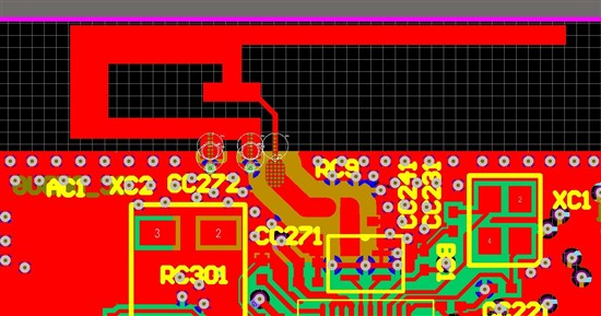
    Now I have changed to a wider microstripe, using the 2nd inner-layer for the reference ground. Here is a screenshot:

    I have ordered the board now, and another board for impedance measurement as well. I will update this thread after I test the boards. 

    However, I have a quite tense board area so I cannot copy too much from all the related reference designs. But I guess the most tricky part is the microstrip. If we use different stack-up for the board, the width of microstrip should be refined. But the guidelines for that is not documented in the reference designs from TI. 

    Another thing is, the output impedance of RF_P and RF_N pins is 69+j29 ohms, I have no idea how to calculate a microstrip for them.

  • You can download Appcad (from Agilent/hp) for Microsrtip calaculations. It is free of charge.The following is the link.

    http://www.hp.woodshot.com/

    Thanks,

    PM

  • HI, PM.

    Thank you very much! That is a really good tool!

  • Hi Igor and PM

    It has been a long time since I posted this thread. Now I have got the boards and done a few measurements and now have the time to update something.

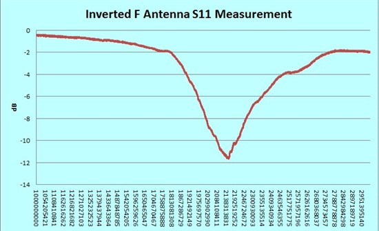
    The microstripe I designed (although it looks a little bit "strangely" wide) has an impedance of about 57 Ohms when I did the Time Domain Response measurement. And it has a return loss of lower than -10dB for quite a long range in the S11 measurement. So it looks like a good microstripe design.

    But when I measured the S11 of the Inverted F Antenna, its central frequency locates at 2.14GHz (which is quite far away from 2.4GHz). The S11 at 2.4-2.5GHz is not as good as what I see from the Design Note DN0007. Here is a screen shot of its S11:

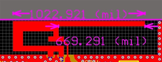
    What should I do to get the right central frequency and a better S11? To shrink the length of the antenna (the 669mil part)??

    Thank you very much!

  • Hi Jinkang,

    If you have several boards I would start to experiment with shortening the antenna length (keep in mind that it is hard to add length if you take off too much :-)).

    Another option would be to investigate the complex value of S11 in a smith chart, and try to tune the antenna impedance with components. I see you have put in placeholders for both a shunt and a series impedance. A nice and free smith chart calculator can be downloaded from Fritz Dellsperger's homepage.

    One issue with the antenna which was not visible in your first figures is the ground plane to the right of the antenna. This will probably affect the antenna impedance. Preferably the antenna should be placed without ground plane on either side, but if that is not possible the distance between the antenna and the plane should be much bigger than in your design.

    I would also not recommend thermal releif on the antenna ground connections.

    /Fredrik

  • Hi, Fredrik

    I really appreciate your suggestions!! 

    To shorten the antenna length with the boards I have is much straight forward. I will try the impedance matching as well. Since I am going for a second version of the board soon so I would like to try to shrink the length of the antenna.

    As for the ground plane on the right side of the antenna, I have a tight board area so may not be possible to remove that part. Of course I will try. 

    About the thermal relief on the antenna ground connections, I followed the design from CC2430-CC2591 Reference Design. Do you think I have to remove the relief there?

  • In the CC2430-CC2591 reference design there are not thermal reliefs on the antenna ground connections as in your design. The ground connections should be solid between the antenna and the ground plane.

    /Fredrik