This thread has been locked.

If you have a related question, please click the "Ask a related question" button in the top right corner. The newly created question will be automatically linked to this question.

cc2540 PCB design help

Hi

this should be bee board [url]http://www.seeedstudio.com/wiki/Bluetooth_Bee[/url] with TI cc2540/cc2541 bluetooth low energy MCU [url]http://www.ti.com/product/cc2540&DCMP=LowPowerRFICs+Other&HQS=Other+OT+cc2540[/url]

I probably made design mistakes and will be glade to hear from you
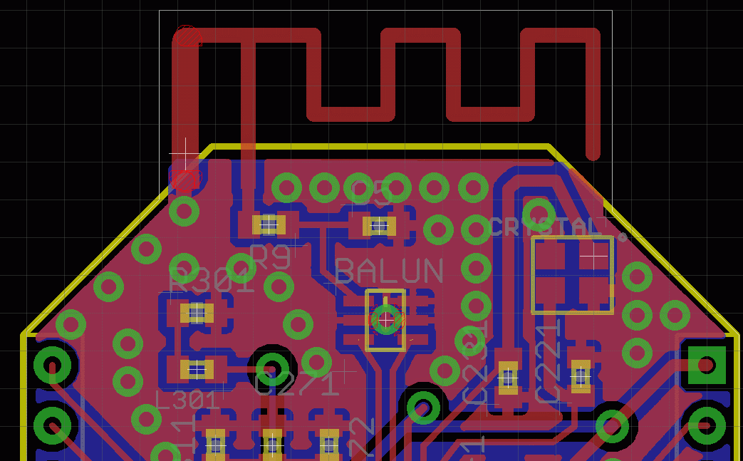
1) I design the PCB antenna from spec [url]http://www.ti.com/lit/an/swra117d/swra117d.pdf[/url]
DRC return overlap error of some antenna parts, corner and connection
 what to do with it? is the antenna connection is wrong?

2) balun part [url]http://www.ti.com/lit/an/swra380a/swra380a.pdf[/url]
this part probably need via under, as you can see the 20 mil via is little bit big and over three pads all ground.

DRC return overlap and clearance errors, can I ignore it as it is overlap ground pads? is the via really needed?
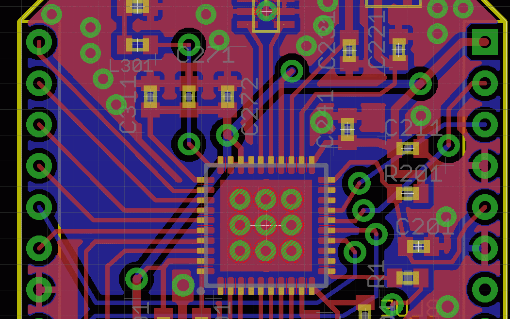
is the via under the MCU should look like in the picture?

any suggested via size (the PCB house "batchpcb" have 20 mil drill limiting, should I change PCB house?)
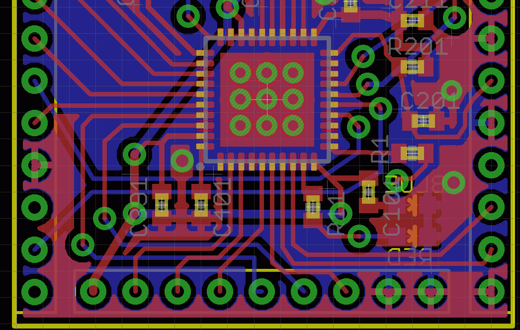
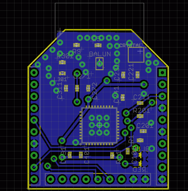
the board is two layers, both are GND plated? is it ok? is there enough GND plate in my board?

isolation 8mil , copper top and button 0.035mm, isolation layer 1.5mm, total 1.57 mm, from readme file of mini kit "PCB DESCRIPTION:4 LAYER PCB 1.6 MM", is it ok?

add some vias between top button ground layers, is it enough? more than needed?

is the distance from CC254x to balun is too far enough? if so what should I do to keep the same distance and still to make it work?

any other issues you see?

BR

  • natanel,

    You have a good start, but there are some issues that I can see from the images you have included. First let me answer the written questions

    the board is two layers, both are GND plated? is it ok? YES, is there enough GND plate in my board? NO, there are too many cutouts in the ground

    isolation 8mil , copper top and button 0.035mm, isolation layer 1.5mm, total 1.57 mm, from readme file of mini kit "PCB DESCRIPTION:4 LAYER PCB 1.6 MM", is it ok? YES

    add some vias between top button ground layers, is it enough? more than needed? Not yet

    is the distance from CC254x to balun is too far enough? Yes, it needs to be exactly the distance used by the balun manufactures. if so what should I do to keep the same distance and still to make it work? Copy the reference design for the balun

    any other issues you see?

    You need to make your ground plane a ground plane, that is you cannot have traces in the ground plane (at minimum no cutout under the RF section)

    Regards,
    /TA

  • Hi Natanel,

    I do also have a couple of observations:

    - You have a VDD trace on the bottom layer going underneath the RF traces, this is a big no-no.

    - The antenna is too close to the ground plane. Check the distance in application note AN043

    - I would change to 0.3mm vias. Then you will be able to make the layout a bit tighter and more tidy, the via underneath the balun will not be shorted to all the balun pins, and you can add more ground vias. (If BatchPCB does not allow smaller vias you could for instance use Seeed Studio' Fusion PCB service. I have tested Seeed myself, it is very good)

    - The decoupling capacitors should preferably be even closer to the power pins

    /Fredrik