This thread has been locked.

If you have a related question, please click the "Ask a related question" button in the top right corner. The newly created question will be automatically linked to this question.

Inverted F Antenna for CC2540

Other Parts Discussed in Thread: CC2540

I've designed my first pcb with an inverted f antenna solution and I'm having problems getting it to communicate to the iphone test app designed by TI.  I have a keyfob pcb that connects fine.  Both the keyfob and this design are programmed with the same code.  I was hoping you guys could take a look and see if something obvious is wrong.

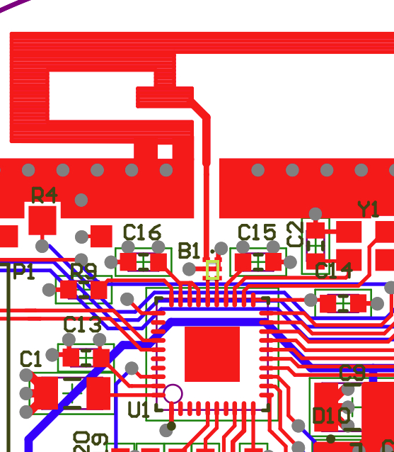
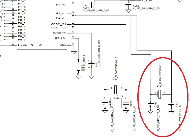
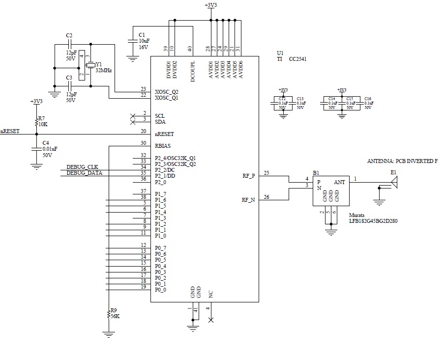
I'm not an RF or antenna expert. I've followed the design notes and I'm using a Murata Balun documented here.  I've attached a screenshot of the pcb layout. The area in the green box is where the balun sits.  Pins 2, 5 and 6 are connected to ground.  Pins 3 and 4 are connected to pins 26N and 25P of the CC2540 respectively. Pin 1 is connected to the antenna design.  The balun is as close to the chip and antenna as possible. There is a power plane and ground plane in the middle layers that is not shown in the image below. The planes do not extend under the antenna.

I don't have a way to measure the antenna impedance. Although I would have assumed that a weak signal would have at least connected to an iPhone when the device is within inches. 

Any help in debugging this would be great, thanks!

  • Jonathan,

    There are a few comments to be made out here with regards to the overall layout of the board. You should read the following article. It gives some good info about do's and don'ts while laying out the RF boards. (http://www.ti.com/litv/pdf/swra367a)

    Having said that, is there a way for you to verify if both the crystal oscillators on your board are functioning?

    Also, can you connect your device to SmartRF Studio and perform basic RF communications with the keyfob? You could follow the basic RF testing document to perform basic RF tests (http://www.ti.com/litv/pdf/swra370)

    You might need two CC Debuggers. One for your board and the other for the keyfob. 

  • I did a design similar to the TI Dongle. Of course my antenna is not matched as the one on TI dongle, I checked that with a network analyzer, and therefore the performance is much worse. What I don't understand is the following:

    I can establish a connection between TI dongle and Keyfob and read out characterstic values from the keyfob using BTool
    When I do the same with my custom built device (which is flashed with the same software as the TI dongle) then I can also establish a connection with Keyfob and I can read a characteristic Value. When I try to read another one (or the one I read before again) then my device hangs up. Could it be that my crystal is worse and because of that synchronization is bad? Or do you have another idea where the problem could be?

  • It could be possible that your crystal is worse and hence you lose sync.

    What crystal are you using in the board?

    Also is it possible for you to remove the 32.768kHz crystal and drive the XOSC32K_Q2 pin with a 32.768kHz CMOS clock, while leaving the XOSC32K_Q1 pin floating. Then try running the same sequence. If you are able to re-read or read something else. This would be a good indicator that the 32,768kHz crystal oscillator components need to be revisited in your design.

  • Hey Chatto, Thanks for the reply.

    Can you explain what the second oscillator on the TI Keyfob is doing? The USB Dongle omits this oscillator, and I'm wondering if this is truly necessary.  My board lacks this component, so perhaps this is what's causing the problems.

  • The 32kHz oscillator is required if one is to use power modes. i.e. for power management, when the device is in sleep mode it runs the ultra low power 32kHz oscillator, rather than the 32MHz oscillator that is functioning during active mode.

    The reason the CC2540 USB dongle does not have a sleep crystal is because, it is constantly in active mode when connected to a USB port.

    There is an internal 32kHz RC oscillator. However, the accuracy of this oscillator is not sufficient for BLE timing requirement and hence can't be used when using the device for BLE mode, where the device is in sleep for large durations of time, almost 90% of the time or more. Hence it requires an accurate clock which the 32kHz crystal oscillator can provide 

  • Ok, so I just hooked the board up to an oscilloscope and measured the 32Mhz oscillator.  All is well.  I compared this signal to the keyfob's oscillator and it looks the same, if not better. 

    I am not use power modes on my device, and it is turned off on the compiler.  I tested this by removing the 32khz oscillator from they keyfob and programming it with my current code, and it still works.

    I've also installed the packet sniffer and smartstudio.  Packet sniffer shows incoming packets from the keyfob, but nothing for my device.

    Any other ideas to check the functionality of the antenna to see if it the signal is actually making it out there?

    Thanks

  • Further investigation...

    I probed the RF_P and RF_N lines on the keyfob, and noticed a 6 pulse square wave occurring when the keyfob is advertising.  
    Probing my device, I do not see this signal. I merely see an initial pulse when the device is powered on.  

    Both devices have the same firmware, so this leads me to believe that it is not an antenna issue, since the signal is not even leaving the CC2540 and going to the balun antenna component.

    My full schematic for the CC2540 component is below. Other than a few caps being different, I can't see any difference between it and the keyfob

  • Are you able to discover the device?  But not able to connect to it?

  • I'm not able to discover or connect to it.  It seems as if the signal isnt even making it out of the chip. I placed probes on the RF_p and and RF_n pins and don't even see the 6 pulses that I see when probing the TI Keyfob.  Odd, because they are running the exact same code

  • Hi Jonathan,

    Why have you put a 10uF cap on the dcoupl pin? This is the output of the internal LDO and using another value than the recommended 1uF can make the LDO unstable which will lead to horrible things (like no RF).

    Apart from that I would highly recommend to follow the decoupling scheme from the reference designs, both due to stability, but also RF performance like spurious emission (it is unlikely that lack of decoupling is the root cause of your problem).

    I assume you have connected the ground pad (EGP) of the chip to the ground layer with several vias?

    /Fredrik

  • Do you have a ferrite bead on your VDD line?  I didn't see one on your partial schematic.  But this ferrite bead is needed to filter out high frequencies when advertising and making connections

  • Jonathan,

    Agree with Fredericks comments here. You should follow the Layout Review Document. It has a ton of info which will help you better layout your board.

    Can you:
    1. Check the voltage at the RBIAS pin
    2. See if your board is able to work from SmartRF Studio. I'd like to see if it is able to transmit a continuous waveform. This would tell us two things 1. For all the short comings of the schematic/layout the board is still functional 2. Verify the debug connections

    Also, do you have more of your boards? sometimes one board gets compromised while being handled. Can you try it on other boards?


  • Fredrik, actually the ground pad is not grounded. Is it grounded internally? the next rev will definitely have it grounded. I'm going to change out the 10uF cap to 1uF, but unfortunately I wont be able to ground the center pad.

  • Hi Jonathan,

    That would definately explain why it does not work. I thought maybe the vias were not visible in the layout since you have a pin 41 connected to ground in the schematic. On a board with similar problem i drilled a 4mm hole through the PCB in the ground pad and strapped the EGP of the chip to surrounding ground plane on the bottom layer.

    The EGP is not connected to any other pins internally (which pins would that be?).

    /Fredrik

  • Hey Guys, 

    So it's been a couple of days and I finally gave up on the board.  I started replacing component after component and nothing was working.

    I assembled a new board by hand, hand soldering the bare minimums (chip, balun antenna, bypass caps, decouple cap, rbias, debug header, etc).  I was mistaken in my post above when I said there were no center vias.  (I didn't design or assemble the first board).  

    I made sure to solder the center pad via the back side and enough flux to make it flow.  In the end, the chip booted, programmed and advertised perfectly. I could connect to it, adjust color led, etc.

    In the end, I really don't know what was wrong with the initial board. It could have been that the center pad was not connected by the guy who assembled the board, or a pad disconnect somewhere.

    Regardless, thank you all for your support.  I'm sure I'll have more questions as I dig deeper into the ble stack.

    Thanks again,

    Jonathan