This thread has been locked.

If you have a related question, please click the "Ask a related question" button in the top right corner. The newly created question will be automatically linked to this question.

matching network & layout for cc1101-q1

Other Parts Discussed in Thread: CC1101-Q1, CC1101

Hi,

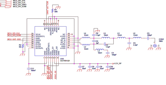
1. cc1101-q1 has a different footprint from the regular cc1101 - So does the layout of the reference design need to be modified to suit the -q1 part?

2. Also, handling 0402 components is extremely difficult. A 0805 inductor with >1GHz SRF is attached. can this be used for the matching network?

3. Similarly, please suggest 0805 type capacitors which can match with your circuit.

Thanks in advance,

Regards

411351553_MLRF0805.pdf
  • Hi,

    A follow-up query.

    The reference design of cc1101 recommends the use of a crystal. But, I am more familiar with crystal oscillators.

    1. How do we decide where to use a crystal oscillator and where to use a crystal?

    2. What circuitry is involved in realizing with a crystal oscillator and what circuitry is involved with a crystal?

    3. Can I switch my circuit to a crystal oscillator instead of a crystal? Then, what are the circuit changes/precautions involved?

    Regards.

  • Hi Mir,

    I can provide a reference design specific for the Q100 versions.

    As for your other questions we have not done any analysis, so I can not really comment.

    Regards,

    Klaus Seiberts

    3513.Reference design.zip

  • Hi Klaus,

    Thank you for the reference design.

    I checked with Kemet site for different sizes of 3.3pF capacitor that is used in the reference design.

    6866.3p3pF_1.pdf

    All of the identified parts are close to the specifications of the part in the reference design.

    Is there any other issue that we need to address for selecting this part?

    or, can i directly use a 1206 sized capacitor?

    Thanks in advance

  • Ensure the total reactance is the same with the 1206 cap as it was with the 0402 cap. 1206 caps have more ESL than 0402 caps. Also make sure tolerances, voltage ratings, etc are the same or better 

    Eric Hooker

    RF consultant

  • Thank you for that  input.

    As I checked on those lines, for the 915MHz operation, C1 and C3 (100pF each) were having their SRF very close to 1GHz based on the reference design (from one of the earlier posts).

    Would that be a problem?

    I was unable to save the datasheet from the recommended manufacturer's site or I would have posted that here.

    Also, is it required that the copper trace be a 50ohm transmission line between all these matching components? or is it that these components effectively form the 50ohm matching impedance? If the latter be the case, from which point is the 50 ohm effective?

    Thanks in advance.

  • For 915 MHz, C1 is a bypass cap and C3 is a coupling cap.  It's desired for those caps to be self resonant near the frequency of operation. Note: the resonance of C1 will be changed slightly due to the ground via inductance.  I pasted the 915 MHz suggested schematic below.

    For your 2nd question, 50 trace is used at 50 ohm points in the matching network -- such as at the SMA connector or on the input and outputs of the Tee LPF.  Otherwise, an appropriate trace width is used at other points within the matching network but not necessarily 50 ohms.  For example, since C1 is a bypass cap, ideally a lower impedance trace would be used.  Of course, PCB real estate is always an issue so that must be considered as well.  All of this can be modeled with a linear circuit simulator and/or EM simulation if desired.

    Best Regards,

    Eric Hooker

    RF Consultant

    www.linkedin.com/in/erichookerrfconsultant 

  • The pasted schematic got lost.  Here it is again:

  • Note that a trace has to be longer than 1/10 of a wavelength as a rule of thumb to actually behave like a 50 ohm line.

    - The impedance between the components in the balun is far from 50ohm so no 50hom lines are required.

    - The distance between the components are normally very short and hence the width is not an issue.

    If you need to use another component size than 0402 I would recommend you to EM simulate your layout (typically the balun/ filter part) and compare the result with simulations on the CC1101 reference design. A lot of customers uses 0603 components with minor modification to the BOM but more care has to be taken with larger components.

  • Hi TER,

    I ran a quick simulation to show that traces will behave as expected below 1/10 of course depending on the frequency.  Attached is a comparison (linear versus EM) of a 0.083 wavelength line at 900 MHz and it indeed acts as expected.  

    I agree that the traces should be EM simulated to be sure and of course tested in the lab.

    4150.600mil MLIN versus SONNET sim.doc

  • Oops, I meant 1/10 of a wavelength above.  

    Eric Hooker

    RF Consultant

  • Thank you all for your inputs. I am incorporating them in the layout.

    I am a beginner to RF systems - so please tell me how the design for the Balun is carried out. Also, what is the role of the T filter? Is it really a T-filter? How is it designed? How do we arrive at the different component values?

    Are there any books to refer?

    Thanks in advance,

    Mir

  • The balun for CC1101 is covered in some detail in http://www.ti.com/general/docs/litabsmultiplefilelist.tsp?literatureNumber=swra168a

  • The LPF provides out of band rejection.  I referred to it as a "Tee" because it has a "T" shape rather than a "pi" shape.  There are many books on RF and filter design.  "RF Circuit Design" by Christopher Bowick is used by some engineers new to RF.

  • Hi,

    I was using the reference design layout for the cc1101-q1. Some of the pads are 0.5mm pads with 0.254mm drill.

    My PCB fabricator is finding it difficult to fabricate these dimensions and is comfortable with a 0.7mm pad.

    1. Is the size of the pad/drill important?

    2. If I use a larger drill and larger pad, would there be any functional implication/trade-off?

    3. How is the RF performance affected with larger drill/pad?

    Thanks in advance.

    Regards.

  • I doubt that the RF performance will be affected too much.

    But if the pad is increased in size the amount of solder paste should probably be adjusted to ensure good soldering but that is something your PCB manufacturer should know about and adjust.  

  • Hi,

    Thanks for the input.

    But, what about via pads and corresponding drill pads? would a 0.5mm via pad with 0.25mm drill be different in performance from 0.7mm via pad?

    Thanks again.

  • TER said:

    I doubt that the RF performance will be affected too much.

    But if the pad is increased in size the amount of solder paste should probably be adjusted to ensure good soldering but that is something your PCB manufacturer should know about and adjust.  

    Hi TER,

    Thank you for the reply.

    I was seeing that the cc1101 datasheet says of 5 drills under the IC and the reference design of cc1101-Q1 shows 9 drills. 

    Can I put 4 numbers of 0.7mm drill under the IC? Will that suffice?

    What is the purpose of putting the drill pads under the IC? Is it to increase the contact for getting a better electrical ground? or is it for better thermal dissipation to the ground?

    Thanks in advance.

  • Hi TER,

    Thank you for the reply.

    I was seeing that the cc1101 datasheet says of 5 drills under the IC and the reference design of cc1101-Q1 shows 9 nos. of 0.5mm drills. 

    Can I put 4 numbers of 0.7mm drill under the IC? Will that suffice?

    What is the purpose of putting the drill pads under the IC? Is it to increase the contact for getting a better electrical ground? or is it for better thermal dissipation to the ground?

    Thanks in advance.

  • Normally the thermal pas on the CC products is the ground to the chip and need good connection to ground. CC1101-Q1 is a automotive part with the ground connections through pins so 4 vias (or as many as you have space for) should suffice.