This thread has been locked.

If you have a related question, please click the "Ask a related question" button in the top right corner. The newly created question will be automatically linked to this question.

CC2540 Antenna Matching

Other Parts Discussed in Thread: CC2540

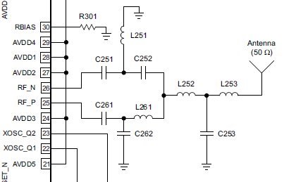
On page 24 of the CC2540 datasheet, it suggests the following circuit to connect to a 50-ohm unbalanced antenna:

  • What should the antenna impedance be looking into the T-network to the left of L252 when there's a 50 ohm load on the other side of the T-network?
  • Is there any way I can tweak the differential impedance seen at the differential RF port on the module (pins 25 and 26)?  Or should I just use the recommended components and layout and assume if my impedance at the right side of the T-network is 50 ohm then the differential impedance at the RF port is correct (correct = 70 - j30)?

Thanks!!  CJ

  • Hi CJ,

    For the balun I would recommend you to copy the values and layout as closely as possible. This should give you a 50 ohm single ended output and correct load capacitance for the CC2540.

    L252, L253 and C253 is used to reduce harmonic emission. I am not sure of what exact impedance you would measure looking into this filter, but it should not be too far from 50 ohm.

    Regards,

    Fredrik

  • CJ,

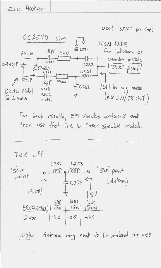
    #1.  I simulated about 11 dB return loss @ 2.4 GHz -- L252, C253 & L253 form a LPF.  Also, at these freqs you have to include the PCB traces and of course component parasitics.

    #2. If you don't use the same vendor for the parts and the same P/N's (they used Murata C's & L's) and if you don't use the recommended layout, you will probably need different component values for best output power & eff.  The device impedance is the complex conj of the 70 + j30 load impedance so it's 70 - j30 which is 82.86 ohms in par with 343 fF @ 2.4 GHz.  The 18 pF caps are coupling caps but could be adjusted. I did a quick sim of the impedance matching parts (L251, C252, L261 & C262) and found 2.2 nH and 0.8 pF worked better.  Of course this was only a simulation.  It is best to keep the L's & C's the same for symmetry which is what I did.  The match return loss was 18 dB at the node that feeds the T-LPF.

    BR,

    Eric Hooker

    RF Consultant 

  • Thanks for this detailed help.  My questions below ask what can I trust and what should I verify? 

    Fredrik K said:


    For the balun I would recommend you to copy the values and layout as closely as possible. This should give you a 50 ohm single ended output and correct load capacitance for the CC2540.

    L252, L253 and C253 is used to reduce harmonic emission. I am not sure of what exact impedance you would measure looking into this filter, but it should not be too far from 50 ohm.

    But I'm pretty sure it won't be right on the money, and my antenna certainly won't be 50 ohms unmatched. 

    Are you saying I should match my antenna to 50 ohms and put my matching network + antenna to the right of the T-filter?  In this case I'm just trusting that everything upstream from my matching network is matched.  Is that a good practice?

    Eric Hooker said:


    #1.  I simulated about 11 dB return loss @ 2.4 GHz -- L252, C253 & L253 form a LPF.  Also, at these freqs you have to include the PCB traces and of course component parasitics.

    By return loss, do you mean S11?  If so, that means about 10% of the power is reflected, which is reasonable.  If you mean S12, something's wrong with the circuit or simulation.

    Eric Hooker said:

    If you don't use the same vendor for the parts and the same P/N's (they used Murata C's & L's) and if you don't use the recommended layout, you will probably need different component values for best output power & eff.  The device impedance is the complex conj of the 70 + j30 load impedance so it's 70 - j30 which is 82.86 ohms in par with 343 fF @ 2.4 GHz.  The 18 pF caps are coupling caps but could be adjusted. I did a quick sim of the impedance matching parts (L251, C252, L261 & C262) and found 2.2 nH and 0.8 pF worked better.  Of course this was only a simulation.  It is best to keep the L's & C's the same for symmetry which is what I did.  The match return loss was 18 dB at the node that feeds the T-LPF.

    Does the T-LPF change the impedance?

    Is there any way to see the differential impedance on my VNA?  Or should I just use the recommended values and layout and assume the left side of the T-LPF is a 50 ohm posit?

  • #1).  Yes, "return loss" means S11 in this case.  11 dB return loss should be improved on if possible.  Actually about 8% is reflected and the mismatch to 50 ohms is 0.36 dB.  I usually design for at least 15 dB return loss.  Download Agilent "AppCAD" -- it's useful free SW.

    #2). The LPF will change the result as I wrote above.  It is a single ended circuit (50 ohms in and out) so you can easily sweep it on a network analyzer.  It's there for harmonic suppression so you can optimize it as needed.  You can add more poles if required for your application.  You can measure diff Z in receive mode but not easily in TX mode.  I believe the impedance is optimized for TX however.  Search the Skyworks website, they have a great app note on differential impedance matching.  I inserted it below.

    3757.Differential impedance matching.pdf

  • Charles,

    I reread your first set of questions.  You should never trust anything is correct especially at 2.4 GHz.  You have a network analyzer and I assume a spectrum analyzer.  The T-LPF can be verified on the network analyzer.  It's nice to have 50 ohm points for testing with 50 ohm test equipment in development & production.  If you need to match your antenna then add the required antenna matching components between L253 and the antenna. 

    I attached some simulation schematics showing what I did last night.  As I wrote there, you will get the best results if you EM simulate the matching layout and then use that information along with the lumped component models to linear simulate the match and LPF.  When I quickly simulated it last night, I only included the traces between L251 & C252 and C262 & L261 using a MLIN microstrip model.

    You can sweep return loss (S11) looking into the match common (C252/L262) node (remove L252).  Of course you can only look at the match in RX mode this way.  The impedance TI supplied applies to TX mode.  One way to confirm the TX match is to measure output power, efficiency, etc in TX mode and compare to the data sheet.  Finally, you may be able to improve performance if you use wire-wound chip inductors such as Coilcraft.  They usually have much better Q's but cost more.  My notes are below.

    Regards,

    Eric Hooker

  • Hi Eric,

    I would like to add a RF switch(PE4259, www.psemi.com/.../pe4259) on the pin1 of a balun (2450BM15A0002, www.ti.com/.../swra297b.pdf) of CC2540. As I am new to impedance matching and EM simulation, I do not know whether I need to add a matching network between the pin1 of balun and the extra RF switch? and how to make it ? Is there any reference design regarding adding RF switch with the same Tx power efficiency?

    I find your note and think it is a good start to learn from scratch. First, I try to do ADS simulation on the first part of your note about differential matching network. As I do not how to fill MLIN microstrip model (W or L), I short it. I keep default values of Q= 50, Rdc=0 Ohm for INDQ and default R=1 Ohm, L=1nH for SRLC. The S11 (on the match common point of C252 and L261) of -18 dB occurs by 2.8nH and 0.8pF rather than 2.2nH and 0.8pF that you mention. Do I miss something on simulation?

    Best Regards,

    Ted
  • Hi Eric,
    I'll answer you in the new thread you started, e2e.ti.com/.../411643

    Please try to avoid duplicating posts.