This thread has been locked.

If you have a related question, please click the "Ask a related question" button in the top right corner. The newly created question will be automatically linked to this question.

MIFA antenna issue

Other Parts Discussed in Thread: CC2540

HI,

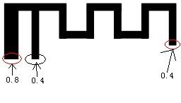
I want to add PCB MIFA antenna, such as CC2540 USB dongle.

My PCB is 0.4mm 2-layer baord thickness, dongle is 1.6mm 4-layer baord thickness.
I reduce the antenna  linewidth size of 0.1mm as Figure, is this correct?

TKS&BR,

Jingle

  • Jingle,

    Keep the line width at 0.4. To compensate for PCB thickness you may vary the length of the radiating end of the antenna. Follow the app note on Small Size 2.4GHz PCB Antenna

  • Dear TI,

    I would like to implement a MIFA on a PCB that's thickness is between 1.5-1.6 mm.

    The placement of the antenna would be on the side of the PCB, but from each side (except the free one) ground layers and other components would sorround it.

    Can you please provide information on how the antenna should be realized?

    Thank you!

    Tamas

  • You will need to push the GND layers and components as far away as possible from the antenna to reduce the influence they will have on the antenna.

  • Thank you for the fast response!

    Unfortunately the application is lacking free room, approximately how much would it degrade the performance of the antenna, if the one in the reference design http://www.ti.com/lit/an/swra117d/swra117d.pdf would be realized (the 15.2 x 5.7 mm version) - surrounded by components?

    How much should I compensate on the length of the antenna with that thickness (~1.6 mm)?

    Tamas

  • Tamas

    These are rather difficult questions to answer and somethings that are not easily determined either.

    Firstly the performance degradation of the antenna can be best studied in an antenna chamber. For that you'd need the prototype design. In this case you want to know the proper dimensions before you make the prototype.

    So, your next option would be to go to a simulator like ADS and layout yur board there and try and get an idea of how the different components near the antenna affect the antenna radiation pattern. This is a long and tedious process. Hence we recommend to our customers to follow our reference designs as closely as possible and make the antenna area as big as possible and on the edge of their boards, away from other components.

    Now, if you do decide to go ahead and make prototypes, you'll then be able to see first hand the antenna radiation characteristics in an antenna chamber and possibly tune the antenna. Also remember, the length of the antenna is reduced to compensate for resonance frequency damping that happens due to the surroundings of the antenna like plastic casing and human body.

  • One important point to keep in mind. Most of the PCB antenna designs rely on the ground plane of the PCB to serve as half of the antenna. This is why PCB antenna designs can be smaller thjan a full dipole, do not have ground or  power planes under them, and why they are typically placed on a PCB edge. So if you put the antenna traces away from an edge of the pcb you will greatly reduce the performance, especially if the antenna is surrounded by ground or power or traces in general.

    You might be able to create a pcb antenna with traces and/or planes on 3 sides, but the cavity would have to be of a specific size (tuned) for the frequency being used. This tuning process could require multiple redesigns of the PCB to get right or really good (i.e. expensive) simulation software..