This thread has been locked.

If you have a related question, please click the "Ask a related question" button in the top right corner. The newly created question will be automatically linked to this question.

CC430 with JTI Balun and PCB Monopole Antenna no RF communication

Other Parts Discussed in Thread: CC430F5137, CCSTUDIO

Hello everybody!

I am working on the CC430F5137 SoC for a Wireless Sensor that I am developing for my Company (working frequency is 868MHz).

After having prototyped (successfully) all hardware and Firmware using the EM430F5137RF900, I designed my PCBs. 

The same Firmware which correctly works on the EM430F5137RF900 Evaluation modules, does not work on my PCBs. Specifically, everything works but the Wireless communication.The sensors don't communicate between themeselves, neither with the EM430. I cold expect some slight variation in the working frequency due to the antenna mismatch, but I didn't expect that the radios didn't work  at all.

For better understanding the problem here I describe my PCB design.

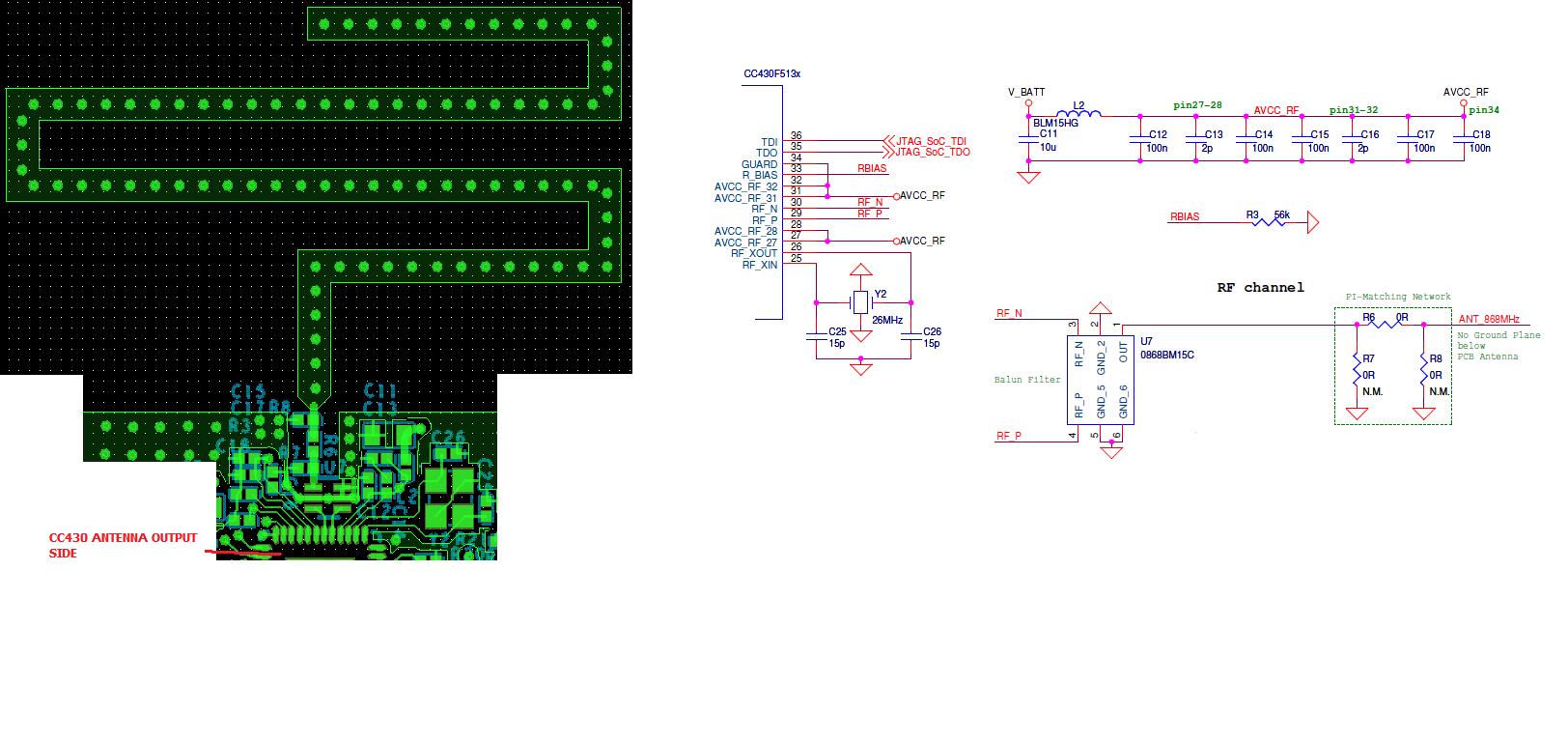
One of the main constraints for the PCB design was using a Low cost antenna, but with good performances, so I choosed the Monopole PCB antenna (single band 868MHz) presented in Design Note DN024. 

I simply followed all hints suggested in the Design Note and, for a future fine tuning, I also added a pi matching network (by now is simply a 0Ohm resistance connecting the Balun to the Antenna).

Because I had some space occupancy constraints, I used the proposed JTI (Johanson Technology) Matched Balun Filter.

So my system is as follows: CC430 RFN/RFP pins - JTI Balun Filter - Pi Matching Network - PCB Monopole Antenna @868MHz.:

Regarding the 26MHz quartz I followed all rules explained in the data-sheet, selecting two 15pF capacitors which, together with the parasytic capacitance on the pin (around 2.5pF) gave a 10pF equivalent capacitance: (1/ ((1/C25)+(1/C26))) + Cparasytic = 10pF.

This capacitance value is ok for both the CC430 and my quartz, whose load capacitance is 10pF.

My question is: what's wrong with this PCBs??

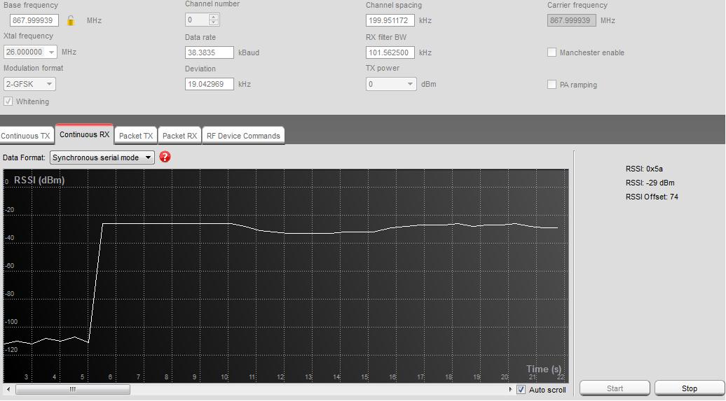
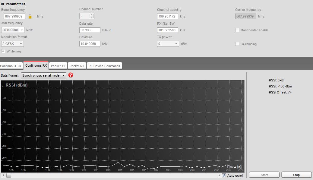
Furthermore I made the following Experiment: I simply downloaded on the EM430 and on my PCBs a Firmware which simply continuously sends  a SYNC word @868MHz, 38.38kbps (sending a Strobe(RF_STX) command).

Using the SMART RF STUDIO 7, configured in Continuous Rx mode I have the following result:

  1. Using both EM430 as sender and receiver: RSSI goes up as soon as I switch on the EM430 continuously transmitting SYNC word @ 868MHz
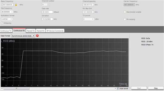
  2. Using my PCBs as sender and receiver: when I switch on my PCB for continuously transmitting SYNC word nothing changes in the RSSI which, strangely, is below the sensitivity level! How can this be possible?

In addition to this, I did another test to better understand if my sensors are, at least, transmitting something:

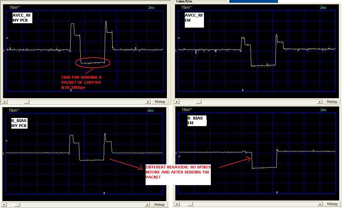
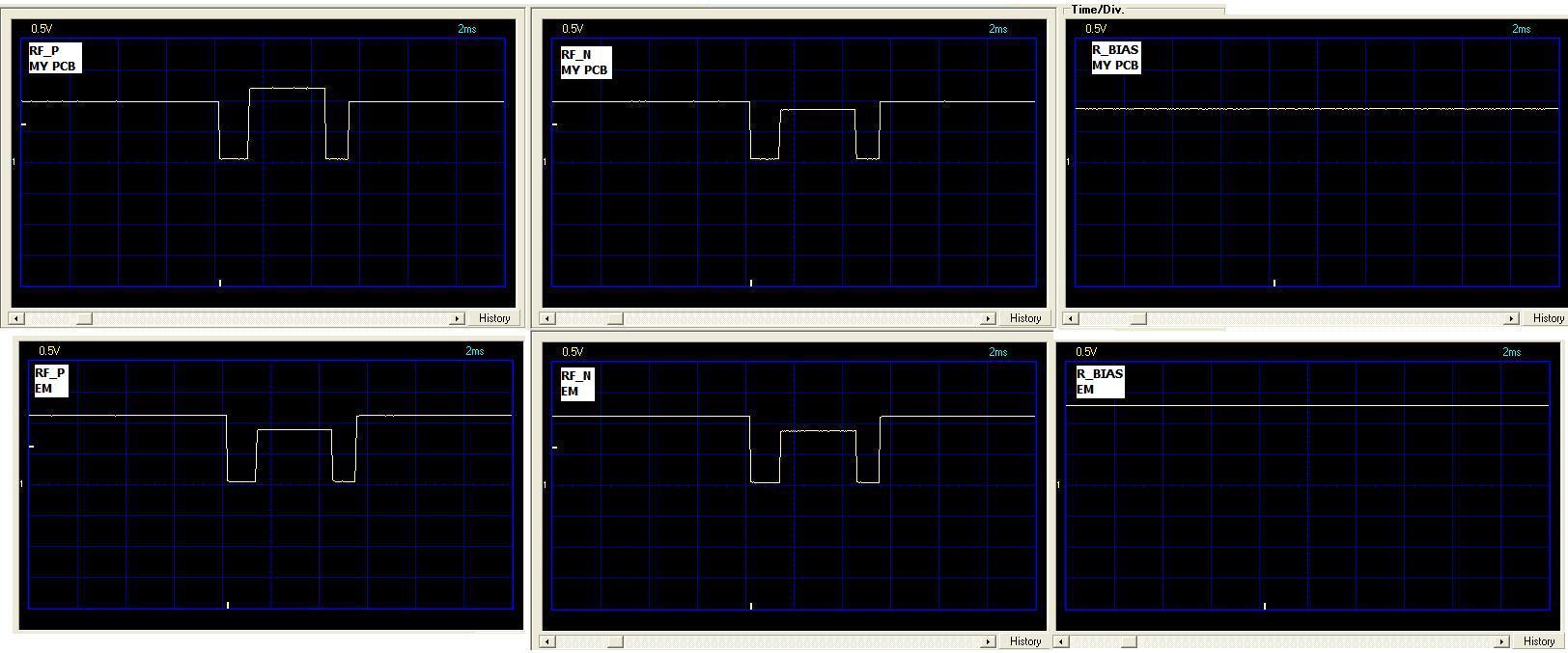
Using my 50 MHz oscilloscope, which I know is not suited for such high frequency signals, but is enough at least to see the signal shape, I checked the voltage values on the RF_N and RF_P pins on both the EM430 and on my sensors when they transmit a 13Byte packet @868MHz, 38.38kbps.

Using both the EM430 and my sensors I have the same signal on the RF_N pin:

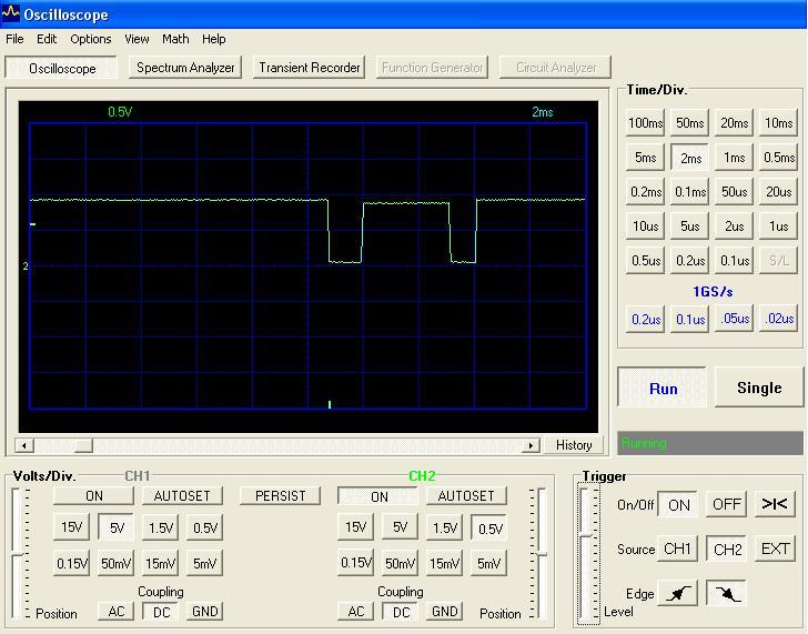
The signal goes down at each transmission, then stands up for the transmission time, then goes down and then up again. The ON time is exactly equal to the time spent for sending the 13 bytes (including Preamble and SYNC).

This seems to me to be good, because at least the output amplifier sends something.

The only difference between EM430 and my sensors is that the RF_P signal has exactly the same shape, but a slightly higher voltage value during the ON phase if compared to the RF_N signal. This does not happen on the EM430 where the signal is exactly the same.

After all this explanation, does anybody have any idea on what's happening to my PCBs?

As I said, I could expect some slight frequency variation compared to the EM430, but not that big! And why the sensors cannot even communicate with each other?

Thanks in advance for your kind help!

Regards,

Claudio

  • My first guess would be to check the oscillator output. Are you using the same oscillator and caps as in the EM board? Use the oscilloscope to verify that the oscillator is really outputting 26Mhz. 

    The antenna will not change the output frequency; although a poorly designed / matched antenna will limit your maximum range. As far as bench-top testing devices within 10 feet or so, it really shouldn't matter much as long as it's connected and not shorted to ground.

    Other things to check would be Vcore voltage while transmitting (should be 1.8 - 2.0v), proper VCC_RF bypass caps, check that RF_N and RF_P are not shorted to ground, and Rbias resistor is 56K.

    Definitely start with the oscillator though - that seems to be a common culprit for no radio communication.

  • Hello Chad and thanks for your quick reply!

    Regarding the oscillator, I already checked it. 

    Specifically I didn't check the quartz output directly (how can I  do this??) but I simply used a MSP430 reference Firmware (CC430x513x_UCS_8) which takes XT2 (my 26MHz oscillator signal) and sends it as output to a Pin. This way I checked that the signal was a 26MHz signal.

    By the way the quartz I am using is the following, and not the one used in the EM430:

    http://www.txc.com.tw/download/products/c/7M-2008-P08.pdf

    The RBIAS resistor is 56k with 1% of uncertainty, as required.

    Anyway I will better check the VCore,VCC_RF during transmission, but as I already explained in my first post, the signal on RF_N and RF_P while transmitting looks the same on the EM430 and pon my PCBs!

    If you have some more hints...they are welcome!

    Regards,

    Claudio

  • Hello Chad, Hello everybody,

    I want to add some more things on my issue.

    I checked all voltages on VCORE (1.79V as expected), VCC_RF (3.4V as expected) and RF_N/RF_P are not shorted to ground. Furthermore during continuous SYNC transmission I noticed that RF_N has a DC value of 0.82V while RF_P 1.3V.

    One more thing is that, checking on the Continuous Rx scope of TI SmartRF7, using as receiver the EM430 and as transmitter the other EM430 board, the RSSI value is high, as said in my first post.

    When I use my sensor as transmitter and EM430 as receiver the only thing I notice is that the noise floor stands at about -110dBm, as expected, and when I activate the sensor for continuous transmission the RSSI value rises to -88/-90dBm.

    This behaviour, unexpectedly, is viewable along a wide range of frequencies: 868MHz +/- 20MHz!

    So, to me, it looks like that my CC430 is sending something, but it look like it is spread all over the bandwidth!

    Does anybody have any idea on what's happening?

    Which test can I do to better understand what's going on?

    Thanks in advance.

    Regards,

    Claudio

  • Are you able to borrow a spectrum to check more on the transmit side?

    When the RSSI on the receiver does not change when you send something your sender probably does not send something at all or it sends on the wrong frequency. With a spectrum you could have set the span wide to see if something pops up somewhere.

    From the software standpoint: Even if your firmware was up and running on the EM, have you checked that the chip is actually in TX and from a software perspective seems like working as intended?

    Have you checked that the VCO/PLL is in lock? See 25.3.3.10.1 in http://www.ti.com/lit/ug/slau259e/slau259e.pdf

  • Hello TER,

    many thanks for your suggestions! Something is starting to move!

    I checked the PLL Locking on my Firmware, which sends a 58B packet each second, having the following behaviour:

    1. When I use it on the EM, the lock detector output, which I related to the RFIFG0 interrupt, goes ON each time a transmission is concluded. Furthermore I read the FSCAL1 register that, as expected, is always set to 0x18.
    2. When I use it on my PCB the RFIFG0 interrupt (Lock detector output) is called only at the first transmission. From that moment on it is not called anymore. Furthermore, reading the FSCAL1 register, its value is 0x3D or 0x2F at the first two packet transmissions, then is always set to 0x3F, meaning that the PLL is not locked.
    What do you think about this? Can it be related to the XT2 quartz or to its capacitances?
    I verified it, using the "CC430x513x_UCS_8" example firmware which is on the CCStudio and it works good on both the EM and my PCBs. Even the capacitances are dimensioned as the data-sheet said!

    Thanks again for your really useful help! And keep waiting for your reply...which will save my design!

    Best regards,
    Claudio

    P.S.: Regarding the Spectrum analyzer I am right going to buy the MSP-SA430-SUB1GHZ. Do you think is a good choice?
  • I have to assume that the firmware will do the same on the EM and your hardware (read/ write the same registers etc) and from this assumption firmware is not the issue.

    It sounds like you have checked the crystal oscillator but it could be useful with a couple of extra tests. Do you have a signal generator with good specs? You can use this to feed a 26 MHz signal in on Q1 through a AC coupling cap to check if this does a difference. It may also work to take the clock signal routed out on a I/O on your EM and use this as your clock source.

  • Hi TER and thanks again for your reply!

    I do not have any signal generator, so I will use my EM for generating the 26MHz clock.

    One question about this: the CC430 clock input pins are RF_XIN and RF_XOUT. How do I generate the clock with the EM? On which pin (RF_XIN or RF_XOUT) of my PCB will I connect the EM clock output signal?

    By the way, I used this TXC quartz as 26MHz source: http://uk.farnell.com/txc/7m-26-000meeq-t/quartz-crystal-26-mhz-10-pf-smd/dp/1866020.

    It needs a 10pF Load capacitance, so I placed 15pF NPO capacitance on both XIN and XOUT pin. I think this is enough for respecting both the CC430 spec (minimum Load cap is 10pF) and the Quartz Spec.

    What do you think about this?

    Thanks again for your help!

    Regards,

    Claudio 

  • By first look your xtal configuration looks correct.

    Try to use your EM as clock source on the RF_XIN pin through a cap (A cap may not be required if the signal is rail to rail)

  • Hi TER!

    I tried to use my EM as clock source, with or without AC decoupling Cap, but got no result.

    Considering this I tried one last test, which I think is the most valuable:

    I unmounted the 26MHz crystal with its capacitances from the EM (which has always correctly worked) and solded it on my own PCB. The result is that I have the same behavior as before! When I look to the RFIFG0 interrupt (Lock detector output), it is called only at the first transmission. From that moment on it is not called anymore. On the EM, as expected, the interrupt is called at each transmission which means PLL is LOCKED on the EM.

    Result: the PLL still doesn't LOCK on my PCB!

    How can this happen??

    ----------------------------------------------------------------------------------------------------------------------

    Considering that this test didn't success I wanted to make a new on to give another look to the main voltages. I kindly and ask you, please, to give a look to the following results! 

    I checked the AVCC_RF/RF_N/RF_P/R_BIAS signals with this test:Using the "Fixed_LT_FIFO" firmware donwloaded from TI website,which sends a packet once you push the button key, I monitored the previous signals at each packet transmission and got a slightly different result on the EM and on my PCB:

                 All signals are without the DC component (Oscilloscope set at 15mV/division; Supply voltage is 3.1V).

    AVCC_RF and R_BIAS behavior at packet transmission (button pressed):


    I notice that the AVCC_RF behaves almost the same way on my PCB and on EM.

    A slightly different behavior is noticeable on R_BIAS.

    Is it possible that this different behavior causes the system not to work correctly?

    • RF_N/RF_P/R_BIAS behavior at packet transmission (signals are with DC component):

    A different behavior is noticeable on the RFP/RF_N signals. On the EM they are perfectly identical. On my PCB there is a different DC value during packet transmission.

    Is it possible that this different behavior causes the system not to work correctly?

    ----------------------------------------------------------------------------------------------------------------------------

    Thanks a lot in advance for your help!

    This issue is really making me crazy....and adding an incredible delay to the project!

    Best regards

    Claudio

  • Hi,

    You say that your board and our EM are identical, is that valid for the layout as well? Could you post your layout so that we can check this as well? How many of your own boards are failing? Have you looked at the soldering and everyting looks ok? Have you tried your XTAL on our EM? Have you tried swapping more compoents between the boards for intstant the chip? How is your power solution, have you tried external power to the CC430 chip?

  • Hello!

    Hereunder I attach a picture of the antenna output layout, using the JTI Balun Filter (0868BM15C0001E).

    Of course the layout is just a bit different from the EM because ,for space constraints, I needed to use the Balun Filter by JTI. Anyway I've followed all layout suggestions I found on TI Deisgn Notes as DN025, DN024.

    The picture represents only the antenna output side of the CC430.

    As Voltage supply I use a Lithium Battery, so Output Voltage is 3.6V. Voltage supply goes directly to the devices without any DC/DC reg.

    In the previous tests I used as voltage supply the MSP430 debugger (msp-FET430uif), and Power Supply was 3.1V. In both cases (3.6V or 3.1V the board does not work). I did not try with other external supplies.

    I tested the behavior on 10 PCB I produced, so this is not a problem of just one PCB. To me it seems not a soldering problem. Probably if it was a soldering problem it would appear on just one board, not on all of them. What do you think about this?

    Regarding my test the only change I made between my PCBs and the EM is the crystal (and its capacitances). I did not change the IC because i think this will damage the board. Anyway considering that my test gave the same unsuccess on 10 different PCBs I produced I don't think it's a matter of the CC430 IC, which, as said before, correctly works in all its part and peripherals.

    Wait for your reply and, if you need further info, just ask.

    Best regards,

    Claudio

  • Hi CHS, Hi TER,

    just to be more precise I just want to let you know that mounting the crystal (ant the related capacitances) which is normally on my PCB, on the EM,the EM works correctly.

    This really confuses me!

    Why, using the same crystal, the CC430 on the EM gets in LOCK while the CC430 on my PCB doesn't??

    This, for sure, it's not due to the crystal and its capacitances!

    Wait for your replies and kind hints!

    Regards,

    Claudio

  • Are you able to check if the ground connection (the die paddle) to the chip is ok?

  • The die paddle is correctly connected to ground: 9 vias connect the IC paddle to the second layer (and also to the fourth layer of my 4 layer FR4 PCB), where I appositely put a continuous ground plane which is spread all over but the Area below the antenna.

    Wait for your further hints!

    Regards

    Claudio

  • Have you tried wiring in a true 50 ohm antenna in your design in place of the PCB antenna? It is possible that the PCB antenna is not 50 ohms and you have some sort of mismatch.

  • Could you post your settings?

  • Hello everybody!

    I want to tell you that after more than a week, I positively solved my transmission issues!

    After all measurements suggested by you and your useful hints and help I simply considered that it was not a problem of settings, Clock, coupling capacitances or soldering.

    in fact it was a production problem! Our suppliers mistakenly mounted a 2.7k resistance in place of the necessary 56k resistance as R BIAS! Considering that it was a 0402 resistance it was not possible to see it by eyes! And, furthermore, the component was sent to our production site in the correct ESD shielding envelope, indicating the correct product code.

    Of course all antenna output stage did not work properly!

    All my indirect measurements on RBIAS gave the same result as the EM, that's why I could not imagine that such a rough mistake could have been done by a worldwide Electronic devices supplier.

    Anyway...everything works fine now..at least!

    Thanks a lot to all of you guys who helped me!

    Regards,

    Claudio.

  • Good to hear you found the problem! I'm sure it's been a frustrating week, but at least you got it and it turned out to be a simple fix (but hard to find). It's always hard reading values of 0402 component, especially in-circuit...

    Good luck with the rest of your project -