This thread has been locked.

If you have a related question, please click the "Ask a related question" button in the top right corner. The newly created question will be automatically linked to this question.

TRF7970a PCB design

Other Parts Discussed in Thread: TRF7970A, TRF7960

Hallo,

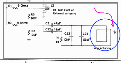
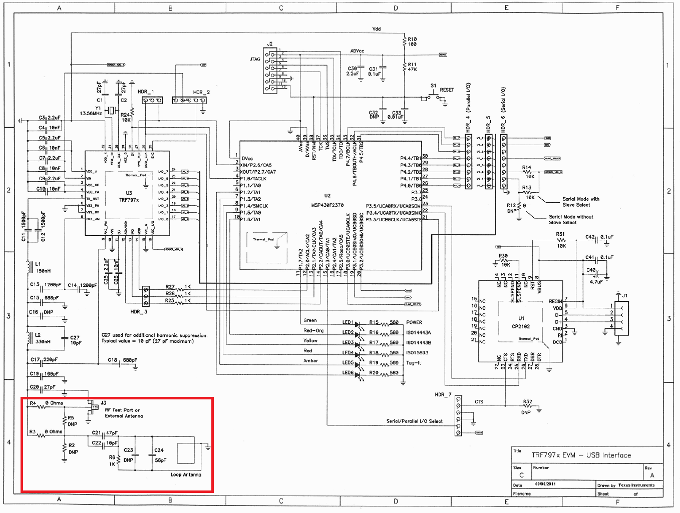
I'm trying develop a PCB layout with the TRF7970a connected to an other MCU via SPI. I stick total to the specifications and the layout from TI. I want to replace the loop antenna with two SMA connector and I want to leave off the RF Test Port.

1) For what are the 0 Ohm resistors?

2) If I leave the RF Test Port off, can I leave also all components with the value DNP off too?

3) To establish a connection via SPI, do I need the connect the DATA_CLOCK (Pin 26) or the SYS_CLOCK (Pin 27) to the my processing MCU?

Thanks and best regards

Flo
  • Flo - 

    you need to connect one side of the coil to ground.(so the way you have it drawn, the bottom SMA would not do anything for you)

    i would recommend you still keep the pads for a connector (you could use U.FL or SMA) for some way to make sure your design in working - that is the intent of the EVM connections you are now wanting to remove - it allows one to look individually at just the output of the impedance matching section, the tuning of the antenna or connect up another antenna coil for experimentation, using a known good system. 

    also see ==> http://www.ti.com/tool/trf7970atb

    regarding your clock question...the EVM and -TB schematics and the data sheet give this answer as well - as name implies, the data clock would be coming from the MCU  to the TRF79xxx for the data communication interface, the system clock is output from the TRF79xxx device and can optionally be used for the MCU in your system - but many MCUs (like many MSP430s, for example) have DCOs so using that output would 100% be your choice.

  • Dear Josh,

    thanks for your reply.

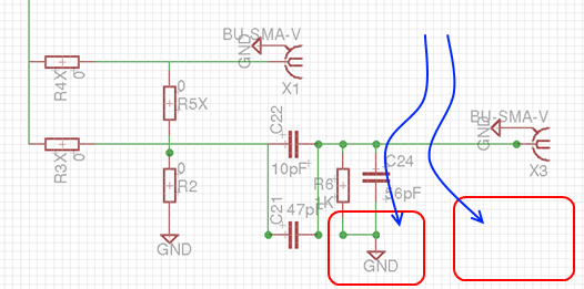
    I have added a GND to the lower SMA connector and I have added a SMA connector as a test port. But I am not quite sure about the pins of the test port. At the TRF7970A EVM PCB it looks like a SMA port, but in the schematics it does not. I am confused.

    And now I have understood the difference between the SYS_CLOCK and the DATA_CLOCk. I think, there were some language difficulties up to now :)

    Thanks and best regards

    Flo

  • Flo - where you are showing X3 and X4, these should just be your coil connection.(i would not put sma or any coax connection there, plus X4 just shorts center conductor to GND)

    the symbols are what the tool uses to indicate a coaxial connection...there are many variations in use, so use this information as new knowledge.


  • Perhaps there was a confusion due to the way the loop antenna was drawn in the reference design schematic, it could be a little bit unclear at first sight:

    The modification in the schematic Josh describes is just to remove the lower SMA connector and connect the line to GND, like this:

    --Victor

  • Dear Victor,

    thanks for your reply. After looking a second time at the schematic I saw my misstake. As you have mentioned it I was confused about the drawing.

    I think my problem is solved now.

    Thanks a lot and best regards

    Flo

  • Good morning,

    I developing a reader of ISO14443A cards and I think that I have a hardware problem.
    First, my reader don't stop to get the same card without front the antenna.
    Second, I set the Modulator control register (0x09) to 0x01 (External clock disabled, OOK 100%). But I have a clock with about 70KHz and I don't know why. Have you any idea?

    Thanks a lot.

    Best regards,

    F.A.Stock

  • you may only have EN2 raised, is that correct? if you raise EN now, you should see it change i think. 

  • I have the EN2 pull-up and EN pull-down tied to MCU. I clear the IO5 and IO3 and set the IO2 and SS. Then I set the EN. So, I configure the SPI communication and call the Initial Settings routine that write Modulator control register.

    Best regards,

  • can you read the register (0x09) back?

  • I read 0x01.

    Do the initialization procedure that I mentioned correct?

    Thanks a lot.

    BR,

    F.A.Stock

  • seems correct - if you are reading a 0x01 back, then you wrote the register. now you can proceed forth with configuring the other registers of the device for mode of operation and your NFC/RFID tasks. 

  • So, I don't understand why SYS_CLK pin still active.

    I have other issues about design, specifically about antenna design. I have here a network analyzer and the document Antenna Matching for the TRF7960 RFID Reader said: "This is done by connecting a RF test connector on three blank circuit boards, one with a 50 load, second with a short (0-W resistor), and third with an open. By using the application board in the calibration, PCB parasitic effects are accounted for."

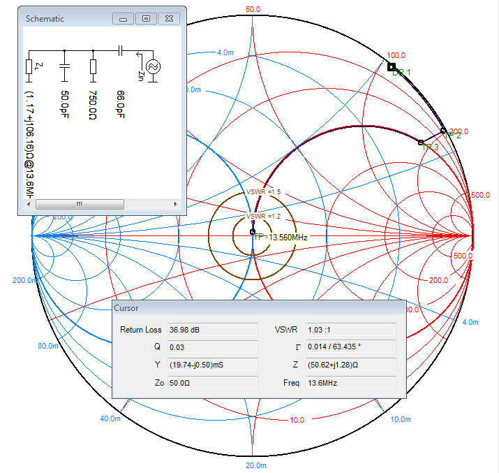
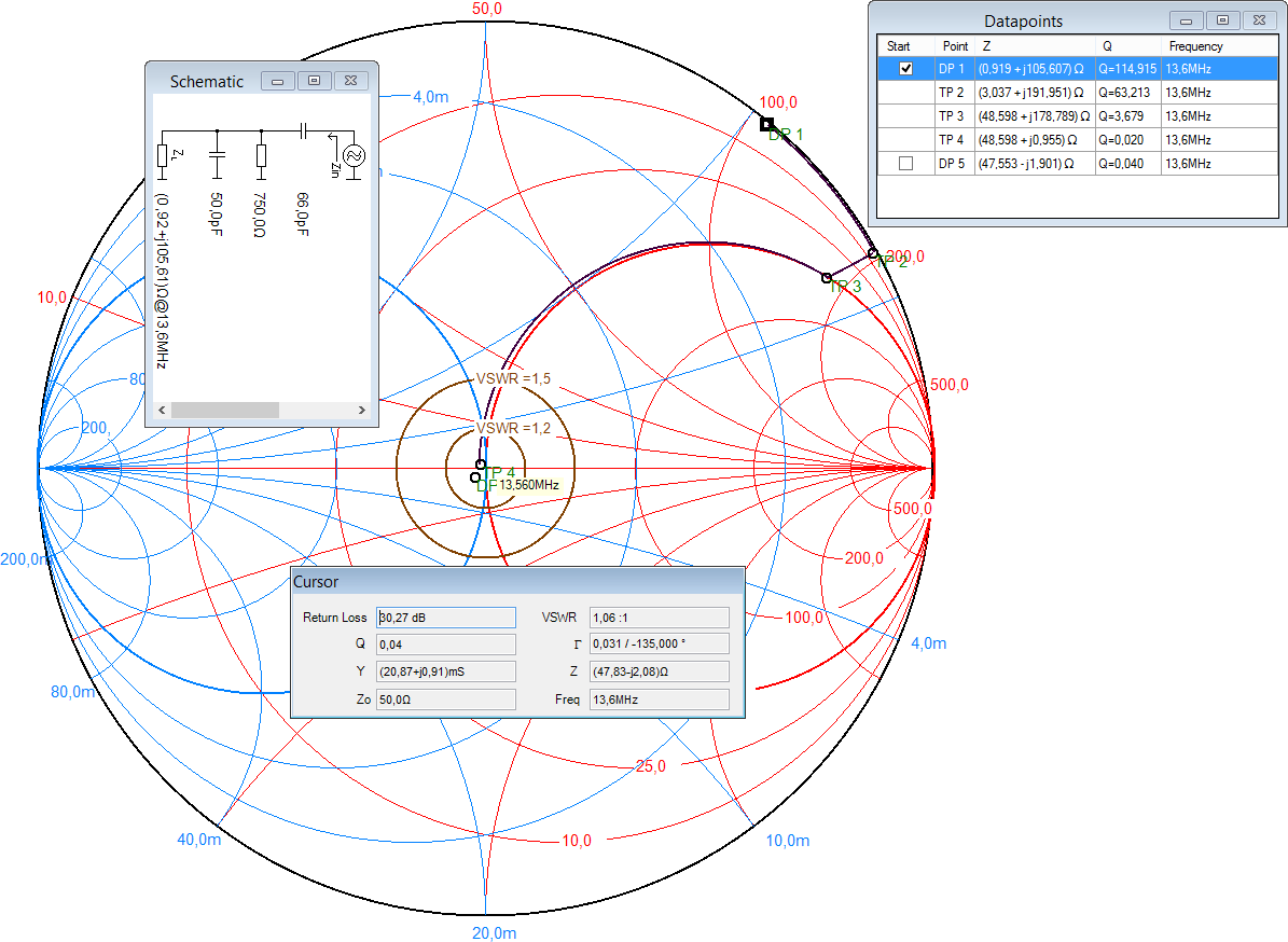
    I did this procedure and I got the complex impedance of designed antenna. Then, I put the value on Smith Chart mentioned at the same document I found the component to do the match.

    With the kit antenna I got good results, seems like datasheet and the Return Loss was good too. My antenna got about (1.165 + j106.157) ohms and when I did the match about (46.5 - j 5) ohms. The return loss was -28dBm at 13.56MHz. Can I improve this? What you suggest to do with the same design? Have you some tip on the measurement process?

    Thanks a lot.

    Best regards,

    F.A.Stock

  • we will look into the sys_clk issue. 

    regarding your antenna - it seems you have ~1.2466uH antenna. (based on your complex impedance value)

    you can check out section in TRF79x0ATB user manuals on the topic too, but here below is the short version, based on your values.

    so then if you want to hit a Q value of about 8 or so, you can multiply the XL by the Q value you want to hit, to get the first value to use of the shunt resistor used for Q dampening. This yields 849.25 Ohms...not a standard value, so go down to 750 Ohms and then plot the tuning solution. This should get you in the ballpark to fine tune from here.

  • I did new measurements and here is the simulation on Smith Chart software and the point that I got after put this tuning solution on board.

    Have you an answer to the SYS_CLK issue? The pin still have a clock between 60Hz-70Hz.

    Thanks a lot.

    Best Regards,

    F.A.Stock

  • Fernando - 

    as long as the EN2 pin is high, the SYS_CLK will be putting out the default osc. frequency, even if B4 & B5 in register 0x09 are 0. We will update the DS to reflect this.