This thread has been locked.

If you have a related question, please click the "Ask a related question" button in the top right corner. The newly created question will be automatically linked to this question.

question regarding the CADSTAR design files (cc2591)

Other Parts Discussed in Thread: CC2591, DXP

Dear  All,

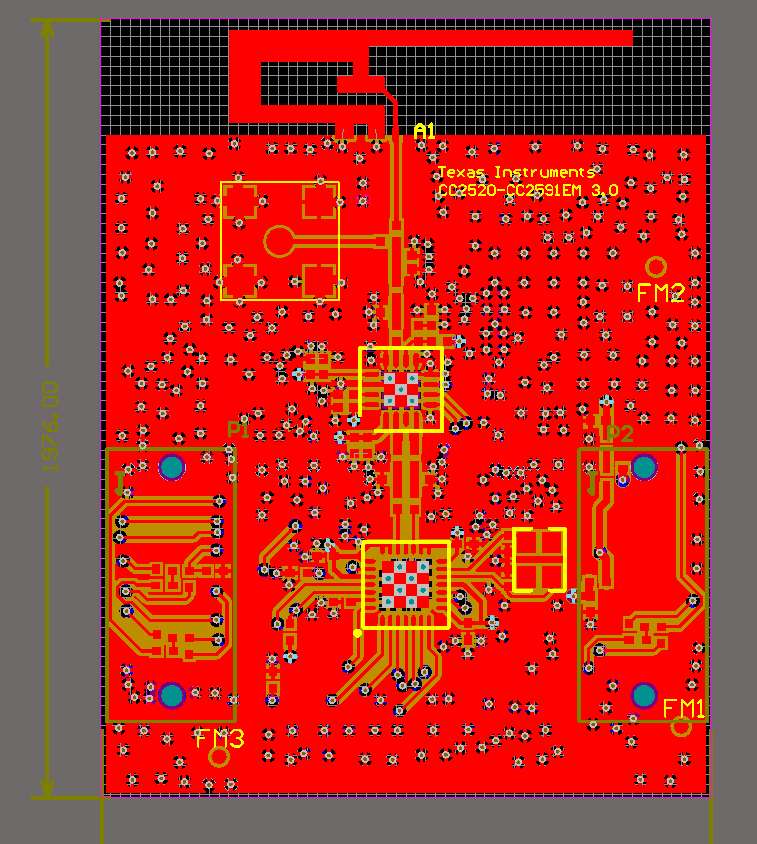
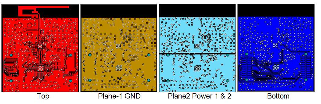
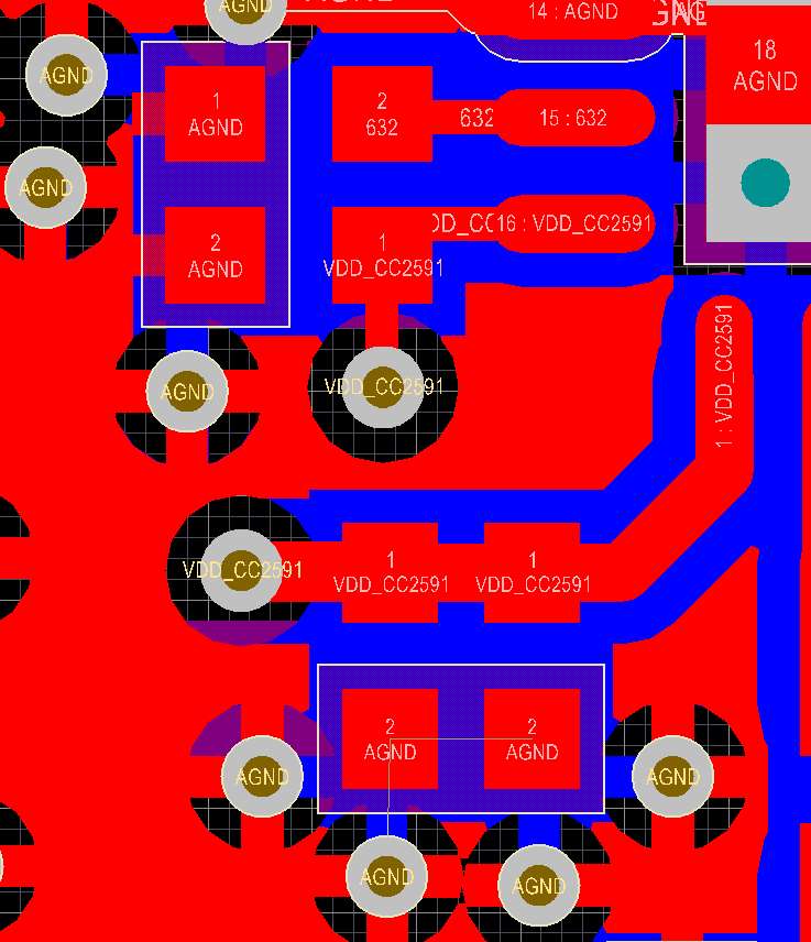
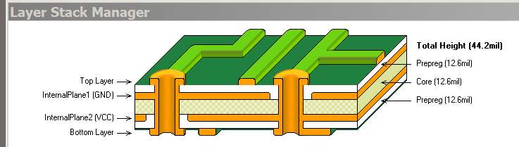
I am having some difficulites understanding the cc2591 design files. No matter what I try, I cannot open the files for editing, only viewing via the latest CADSTAR 11 viewer. How could I edit those, if we do not own a Mentor Graphics editing software? I have Autocad, Protel, Orcad access, but not really worked with the Cadstar or Mentor Graphics software.

Best wishes and a Happy New Year 2010!

Ghasem

  • Pleae include the URL to the Ti files you are trying to open and I will see what I can do to help.

  • Hi,

    The file is a zip file which I downloaded and unzipped by clicking at this URL http://www.ti.com/litv/zip/swru190b.

    I arrived at the above mentioned URL, when I searched for the CC2591 in the part search at the www.ti.com.

    The zip file contains several files, including a .pcb file and some other format files. I wanted to basically make it easy for myself, and take for example the antenna design from the file, since it has a PCB type antenna design.

    Please note that I can open the file with the CADSTAR version 11 for viewing, but cannot copy or edit it basically into another format. I tried also using the PADS software from Mentor Graphics, the latest downloadable version, but their demo software can also convert the .CPA or .SPA file or something like this and read the file then, the same as the CADSTAR viewer, but I could not again edit it into Protel or Orcad format, which is basically what I want.

    Best regards,

    Ghasem

  • I believe I have attached a zip file with the top layer of the CC2591 save as a Protel 28 ascii file and a autocad .dwg file.  Let me know if this work.  i can also convert the circuit to Gerber files.

  • OK,  I have uploaded "DWG_ Protel-Folder.zip" a number of times but do not see where it went.

    DWG_ Protel-Folder.zip
  • I have tried to download the uploaded zip file; there is some form of error coming from a ".Net" or something like this. I anyway could not retrieve the file "DWG_ Protel-Folder.zip".

    May I ask how did you upload, because I do't find an upload file option ?

  • Please ignore my last remark, I was able to download the file right after I sent out the previous response. I will check it out now.

  • Once you click Reply  there is

    Compose | Options | Preview

    above and left of the message you are repling to.  If you click Options you will be given the choice to upload a file or include a link to a file.

    Do you get the error trying to download the file or trying to open it??

  • I was able to use the .pcb ascii protel format file successfully. The file is however not complete. The file has I think the complete top layer data, some of the bottom layer data which is at the lower part of the board is also there, and some middle layer. But the upper part of the file which contains the antenna on the PCB, which I believe must be the bottom layer is missing. Could you also send in the bottom layer?

    I could not use the dwg file. I will try to look at it, but I am not very good with good autocad formats, mostly protel, or dxp protel.

  • The antenna is on the top layer.  I opened the converter file and saw the same thing.  It looks like the polygon pours are lost in the translation.

    The following is the file in Altium (Summer 2009) where it looks like all of the layers are intact including split polygons.  Can you use Altium files or a full set of Gerbers? By DXP do you mean Altium?

  • Ok, here is how it is looking right now. I am able to select the components from the top and bottom both, which are visible. I have turned on all the layers. The green is the mile layer. I had a question also. When I select a component, such as for example, from either of the chips, then I ass a matrix of pads in the inside portion of the chip. Since these are the QFN parts, this is I believe supposed to be like that. But I do't understand that these are running from top layer to the bottom layer, the pads or vias in the inside area of the QFN components I mean, or are they running from top or bottom layer to another layer?

  • Here are the 4 planes. Other than ground vias there are no QFN pads on layers 2-4

  • By the DXP protel I mean the Altium, yes.

    I have not tried before using the gerber files, but please send them in and I will try them out. It could be my solution.

  • I want to go ahead and ask you on the four sides which was posted in your previous response. The thing is I try my board designs double sided, which means I even fit the power and ground on the same two sides, i.e, top and bottom. When I then try to check the interconnections, I mean, if I want to see where the power is located closest to a certain component, I simply press the CONTROL+H keys on my keyboard, when in the protel software, and then I see all the power connections light up, so this is very important when designing. I do't however quite understand, how the four sided PCB works, i.e, top, bottom, and the power and ground in the middle. What are these? I mean, suppose, I connect the power from the power source to the power plane, by placing a via and then changing its properties to start from the power source from the top layer and end in the power plane. Is this the correct way of interconnecting the the suppose 5 volt power supply to the power plane, and thus being able to retrieve this same 5 volt at another part of the board, by placing another via that start from the power plane, and ends suppose at the bottom layer?
  • A common 4 layer board is like this:

    1 ---Top signal Layer with copper pour connnect to ground-----
    2 ------------------------ Ground plane ---------------------------------
    3 ----------------------- +3Vdd Plane -----------------------------------
    4 ------------------------ Ground Plane ---------------------------------

    All vias go through all layers top to bottom. (Yes, it possible to have "blind" vias that go between layer pairs but it costs a lot more.) The nice thing about 4 layers with a power and ground plane is if you need power or ground you just pop in a via and you are connected. You do not have to route traces for power or ground. They are always there by adding a via.  The BIG advantage is the ground plane is continuous, without breaks, because it does not have lines. A continuous ground plane is important at 2.4GHz. If you look at a simple Ti design like a CC2430EM you will see the ground plane on the bottom layer under the RF matching section does not have a single break or line. With more complex designs this becomes nearly impossible with 2 layers.

    If you look at the photo where I zoomed in on the Vdd lines for the CC2591 notice how the Vdd comes from the via, goes to the bypass cap which is grounded with a via, and then to the CC2591. The lines are short, the ground pour on the top, layer 2 and the bottom are not broken by a Vdd trace, and the person doing the layout didn’t have to figure how to route the power all over the board. There is little worry of coupling between devices due to a long Vdd line connecting them which could cause feedback and oscillations. When you route a Vdd line and add a via it automatically connects to the Vdd plane.

    The power and ground plane do not have signal traces on them. All signals are on the top and bottom.

    I will try to up load the Altium files. Which version of Altium do you have?

  • I have attached the CC2591 schematic and PCB files that I converted from CADSTAR. See if they will open in your version of Altium.

    Altium-CC2591-PCB-SCH-DOCs.zip
  • Ok, I will download the file, but now I have another question. Suppose, that in my two layer board, which has become increasingly complex, I insert a power plane and ground plane, i.e, immediately below the top layer I insert a layer, the power plane, and then whenever I need access to say 5 volt or 3.3 volts, I can insert a via from the top layer to the power plane. Then, now, I also insert another layer, the ground plane, immediately below the power plane, and that mean, I will have now the top layer, then the power plane, then the ground plane, then the bottom layer. Now wherever I need access to the ground plane, or the 0 volts basically, or the digital ground, I can insert a via from the top layer to the ground plane. See, the point I was making before about being able to see all the signal lines tied together in for example the software Protel (cntrl+H) in this case, is that, I can see all the pins on a chip which goto the ground just by looking from the top layer, and turning on all layers ofcourse. Thus if I need to see all the pins and lines going to ground, I can just high light it in a second, and find any possible errors. But I do't understand, how can I see an overview of all the lines going to ground or to the power plane, I mean the one's that are using the power plane and the ground plane which I have just inserted, because when I try to just look from the top layer, and I turn on all the layers, I can just see a via indicating that this pin for example on the top layer is going to the power plane, but If I want to see the interconnection from this pin through the via and to the power plane, then how can I see it? Or basically my question is how can I high light all the pins running through the vias to the power plane separate from the rest of the pins? If you could also indicate to me, that I suppose create some form of a list of all the pins which are supposed to run to the power, if it is not possible to highlight them, and then just add or remove from this list, all he power or ground requirements, then it is nearly the samething, but then what is this method called, the net-list?


  • I have downloaded the file. The problem I am having is that the file is of version 6, and when I look at the Altium version that I have, it is version 7.07 or something like this. I have tried to register and download the latest Altium, but I am not sure if this will solve my problem. I knwo this though that I can work with the following files. Files saved in the version "PCB 3.0 Binary file" or  "PCB 4.0 Binary file" from within altium. I can open those actualiy with the Protel99SE as well. But this is weird, because either my Altium version is not 7, or there is some other problem, because the files which are of older version are able to be opened with the designer which is of a later version. Is this not the rule? The later versions support the older versions?

  • Just going back to the original question of how to edit CADSTAR files.

    Please note that there is a freeware called CADSTARExpress (http://www.zuken.com/products/cadstar/downloads/express.aspx). CADSTAR Express provides all the functionality of CADSTAR, limited to 300 pins & 50 components.  

  • The files are from Altium Summer 2009 SP3  (ver 9.1.0.18363 ) which is the most current and is up todate.

    To answer some of your questions:


    The layer order is Top(Layer 1), Ground(2), Power(3), and Bottom(4).  The reason is the RF transmission lines are of a certain impedance. Impedance is controlled by the dielectric properties of the PCB material, the width of the line, AND the thickness of the PCB material between the line and the plane below it. If the power plane is directly under the RF lines on layer 1 then the power plane becomes the RF ground plane which, while possible, is difficult because the Ti chips use the same “ground” for dc and RF.


    All of the vias go from top to bottom. If the via is on net VCC and the power plane is also net VCC the via will automatically attach to the VCC plane2 (3). It will automatically have a clearance gap where it goes through the ground plane(2) and also on the bottom(4) so it does not connect to the copper pour on the bottom which is connected to net ground.


    Look carefully at the picture from the Altium Layer Stack Manager to see this better. My power plane labeled VCC is only connected to +3.3Vdc output of the voltage regulator. You can use a layer instead of a plane where it is possible to use polygons to define different areas connected to different nets (ex.: Net Vdd3.3V, Net Vdd5V,)


    In PCB design (OrCad, Eagle, Altium, etc) the schematic is King.  The schematic defines the interconnects, the foot prints are associated with the symbols here. The net list will be output from the schematic editor. Once the schematic is finished you are nearly done. Once you convert it to layout you will see all of the footprints with fine lines (so called "air wires") between them so you know how to route lines between them. It will not let you connect a line to the wrong pin. If you miss a connection the design rule checker with catch it. If you click a net on the schematic it will light up on the layout. If you click a net on the layout everything on that net on the layout will light up as will the same net on the schematic. (This is where two screens are real nice but one screen with both the layout and schematic works too). This all works provided the schematic is complete, the schematic symbols are accurate, and the foot print pins match the symbol's pins.


    Symbols and Footprints:  The forums are full of people looking for symbols and foot prints. I do not understand this. They are quick and easy to make and every time I use one from an open library I seem to have a problem with it.


    Step 1 is to pick a PCB CAD tool and complete the schematic including symbols and foot prints.

    Let me know if you need help.


  • OK, the help I need right now is the following. I am using Altium so whatever I say here is related to Altium. The design is on double sided PCB, which means there is not power or ground plane. All power and ground run on either the top layer or the bottom layer. Now, what I immediately want to do, is to insert the ground plane immediately below the top layer, and the power plane immediately above the bottom layer, i.e., make it four sided. I do't see the point of completing a schematic right now and taking it to a PCB layout then. But what I immediately want to do after I inserted the power and ground plane, is to shift all the power and ground connections from the top and bottom layers to the power and ground planes, by inserting vias where ever required, and removing the previous tracks to the power and ground which were cluttering up the layout. In order to do so, I need to also define a net, and after defining the related via, I would alike to be able to insert it in a net. I do't know right now how to insert it in a net. I mean I want to define a net in Altium, say VCC3.3, and then assign the via to the net after I have inserted and defined it to be a connection from top to ground. How can I do this? I would also need another for the ground plane. If I can do this, I can then highlight the net afterwards, and thus save myself from any type of possible errors.

    I also have another question, that in case of the connectors, which run through the board, I would however need a pad in a connector defined as the ground, how may I then insert a say, 10 pin connector, in which 8 pins are running to the signal layers top and bottom as before, but now two of the pads in the 10 pin connector go to the power plane? Will this actually be the correct way to go with the PCB layout and later manufacturing?

  • You have a earlier version of Altium so everything is not the same as mine in term of menus or feature but the basic functions are still if you can find them. I can tell you how to do it in Altium 9.1 then we will have to figure it out.

    A good tool for capturing screen shots is at Screenshot32.com   It is free, once set up you press "Print Screen", drag a box around what you want, right click, and it saves a .jpg to a file.

    Adding Planes  under the design tab I have "Layer Stack Manager".  I'm sure you have something like this.

    On a blank part of the lay out area right click, select Option, then select Edit Nets... Here under Net Class add GND, set the annular ring size, hole size, and line width. (ex 40mils, 20mils, 10mils)  Once the nets are established you can go to the next step (If you have a schematic all of the nets would already be here). I'm trying to find a way to add all of the nets to a table to save some work.

     In stack manager I click the top layer, then click Add Plane. Once it is added I double click it add set the Net name to GND.
     Still In stack manager I click the bottom layer, then click Add Plane. Once it is added I double click it add and set the Net name to VCC or what ever you are using. If you want more than one plane on this layer click Add Layer. Later you can select this layer a draw a polygon for each plane and attach each one to a different Net (eg VCC33 and VCC5)

    To add the vias there are 2 ways to go.  Select place, via, and put the via where you want it. Select the via, right click it, and it properties add the name of the Net it is attached to. The second way is to route a line to where you want the via, push the + key and a via will appear, click once to fix it in place. You can push the L key to change the layer you are routing on.

    Lines that are ready routed can be named by selecting them, right clicking, properties, and select the net name.

  • I have yet to download the screen capture tool you mentioned. But about the power and GND plane assignments and definitions of vias. I went through all the steps as mentioned. There is however on thing that I cannot see the highlighted power connections, when I click the VCC net. What I mean is that, I have defined the power plane as belonging to the net VCC. Then in the layout, I have defined vias running from the top layer to the power plane and assigned the via to the net VCC, an then running from the bottom layer to the power plane, and then assigned to the net VCC. I do't understand, when I click one of the vias via (cntrl+H), which is supposed to show the interconnectivity, why I cannot see the power plane and the other via highlight? Have I not assigned the power plane in the layer stack manager to VCC, and then defined vias running to it, and then to the top and bottom layer and also assigned to the same net VCC? Then why am I not able to see them highlight altogether, when click one of the vias?

    This, and my other problem was on the connector pins. As you know, the connector pins run through the board, but only the interconnection to one of the layers is required. Thus in a 20 pins connector, I may want to conenct the first pin to power plane, and not to the top layer, the bottom layer or the ground layer. The how may I do this? I defined the pad belonging to the first pin in a 20 pins connector as connected to the power plane, but when I tried to attach it to the to the VCC net, nothing happened. Sorry about not sending the screen shots, I can send you screen shots like the ones before, but not like the ones you sent in right now.

  • Here is what I see. Cctrl H works nice, I didn't know about it before your posting. On layer 2 you can see the 4 vias connected to Layer 2 (Net GND), on layer 3 there is the clearance and no connection for the GND vias but you can see pin 9 of the 10 pin header is connected to VCC and had clearance on Layer 2 (GND). I just put the ten pin connector down, right click on pin 9 and selected VCC for the net.  The software did the rest.


    If a pin that is passing through the board is not on net VCC or GND it will not connect. There is nothing you have to do. Even when you add copper pour to the top and bottom and attach them to GND only thru hole pins on Net GND will be attached to tese pour as shown below. Note the relief around VCC and pin 10. It is automatic.

  • In a double layer board design, or as a matter of fact, in any board, using the Altium tool, how are we able to add a layer of text, which during manufacturing, shows as white text over a green PCB? I mean I can ask for a green print or layer or whatever that is shown in manufacturing, but how do you make the white text appear over the green layer? Which layer is this and how do we add text into it? I asked from the PCB manufacturer, and they say this is a markup layer. but I could not find the markup layer in the layer stack manager or the board and layers in the options menu.


  • Text on the board is straight forward.  You can add another layer by any name, t will be output as another Gerber file. Just be sure to tell the PCB manufacture which Gerber file is for what.  Some fabs have a map where you enter the layer name for each layer type during the file up load process. The common default is  the layer Overlay and the Gerber files are gto for Gerber Top Overlay and gbo for Gerber Bottom Overlay. The default color for Top Overlay in Altium is yellow. This is the on screen color, what color ink the PCB house applies using the Gerber file is up to you / them.

    Be sure to click properties for each component and set Designator to Visible and set the Overlay layer to on.  You can set the font size globally and when each foot print is selected the global value will be used. Once the footprints are on the layout Global does not change them, you have to do them one at a time via properties.

    You can add additional text by selecting the Overlay layer and then "Place" selecting text which is typically show with the letter “A”. Bar codes, Logos etc are typically meta files.

    In addition to Overlay I also use a un-used mechanical layer to place text on the layout, including designators and notes. I turn this layer on when I plot the circuit to be used as an assembly aide. Since I do not send this layer to the PCB house or included it in the DRC checks the text can be on pads, over components, off the board, and have lines pointing to which component a designator is for if needed in tight places.  whatever I need to do to make it clear and easy to read. On really tight boards I only use this approach and only have a few designators, part number / rev, and of course copy right info actually printed on the board.

    -H


  • OK, so in order to add text, I would need to use a layer. I am not sure what layer to use, but I do't want to use the Top Overlay, because I do't want the board cluttered with all the lines for all the components and devices. I just want to be able to add some text as a guide, or maybe copy right information perhaps. But now I want to ask this. How may I just send the layers to the PCB house, which are required? Suppose, I have "Top Layer", "Bottom Layer", "Mechanical", the rest were not used, and maybe "text layer". Now I know that there are many layers "Top Overlay", "Bottom Overlay", etc., but I do't want to those used in the making of the PCB, thus how may I send in only those which are absolutely necessary?

  •  As a minimum I would expect the following:


    1.) Top Layer with lines, pads, vias, copper pour     GTL

    2.) Bottom layer with lines, pads for through hole parts, vias, copper pour GBL

    3.) InterPlane1 if used  GP1

    4.) InterPlane2 if used  GP2

    5.) Top solder mask   GTS

    6.) Bottom solder mask GBS

    7.) Top Paste mask GTP, you will need this to order the solder stencil, $125 well spent.

    8.) Top Keep Out (generally Mech-13) defining the board edge, it is used to cut the board out of the panel  GKO

    9.) Top overlay for designators and text    GTO


    10.) In addition you will need a drill table and an ASCII drill file (readable in Note pad or other simple .txt editor.


    If your foot prints have a bunch of extra lines on the Overlay Layer edit the footprint and change these lines to a un-used layer so you can ignore them and can change them back if you want them later, or just delete the extra lines. As I wrote before open, library parts often come with extras and problems, I make my own.


  • I would like to go back to our previous discussion, in which I mentioned my problem about not being able to use the Net in the four layer board in order to get the proper board overview. For example, I said, I have a dual layer board, and I attach all the VCC together, then I can see all the VCC connected lined high-light together, even if it is running on both sides of the board. But this is no longer the case, if I introduce two more layer, one ground and one VCC, and then try to route the power lines over those, which means, if I now try pressing ctrl+H, I do't get the proper high-lighted tracks which I should see. I also said I do't know the reason for that, and I have tried defining nets, and including the layers in the Nets, and assigning the vias and the tracks to nets, but even after that, when I click a track which is running through the via to the power plane, to another track or component (on now my two layer board converted to four layer board) and then try ctrl-H on them, I do't see them highlighted, even when they are on the same net.

    What I do't understand is, that if I open the file which was for the Altium (the CC2591 file saved from CADSTAR format to Altium), adn then for example click any via which is running to the ground layer, then I see the whole ground plane high-light, including all the ground vias, and the tracks running to the ground.

    This I have tried capturing via the screen capture tool and attached it. Sorry I am having little bit of problem about attaching the files, I am going to attach them with the next post.


  • Hi, here are the files I was talking about in the last post.

  • The part which I am talking about here, is the one that the file was originally a two layer board, which I had all the signal and power running on the two layers. Thus when I wanted to see an overview of the VCC or GND, I would just run ctrl+H and see them all high-lighted. The file which I have attached here, is the one that I have inserted two more layers. Now there is a GND and VCC plane, below the TOP and BOTTOM layers. If you look closely, on the top I have placed a via running from the TOP layer which is the red color, to the VCC3.3 which is greenish color, and there is also a Net the VCC3.3 net. I hve also run ctrl-H, which is supposed to show the interconnections, thus the all the interconnections on the TOP going to this via are high-lighted. Next, I have a via at the lower part of the screen. This is running from the BOTTOM layer to the VCC3.3, which is also represented by the colors, BLUE to greenish color, the greenish being the VCC3.3 layer, there is also the VCC3.3 Net, which can be seen on the via.

    Now as far as I am concerned, the via on the top of the screen which is running from the TOP layer to the VCC3.3 plane, and the via on the bottom of the screen, are interconnected, one from the top layer to the VCC layer, and the other from the bottom layer to the VCC. But as you can see, when I have tried to check interconnetion between them by running ctrl-H, there is nothing to show me an overview or high-light. Are these not connected then? What may be the problem and how may I solve this design problem I am having.

  • First the bright green items are those with design rule errors, you can turn this off by using Tools / Reset Error Markers

    Most PCB design tools are designed to work off the Schematic which provide the interconnects on a net list making functions like ctrl H easy to implement in software by highlighting all object on a given net. 

    Without a schematic you need to right click every pad, plane, fill and line and individually assign them to the desired Net. I notice that many of the vias in the photo do not have a net label in their center.

    I have created a PCB only file to see what you are seeing.  When I assign lines and vias to a Net, like AGND, and click any on the same Net, on top or bottom, they all light up using ctrl H.

    If I do not assign 2 lines or pads to the same net the software will not let me connect them. One way around this is to change the design rules to permit shorts, which I would not recommend doing. If I add 2 lines while permitting shorts and then add a 3rd line connecting them ctrl H does not work.  Even through they look “connected” they are not the same net. Ctrl H highlights items of the same Net. It does not highlight all items that just happen to be shorted together.


  • I started a new PCB in Altium, by clicking New->file. Next I clicked the layer stack manager and added two more layers planes, as shown in the files I have include. Just before that I also defined the Net called VCC, so that in the layer stack manager I can add the plane called VCC to the Net VCC. Then in the new pcb, I added two vias, on running from the bottom to the vcc plane, and another running from the ground plane to the vc plane. I added the vias to the VCC net.

    I do't get it that why when I click on the first via using ctrl-H, I cannot see both the vias highlight? This time I have started from a fresh pcb, I have clearly defined the layers, and created Nets all from the beginning. Just I have no schematic. I have whatever which is on the pcb in the nets, nothin which is not placed on the net. Clearly, the first via is attached to the VCC plane from bottom layer, and the second one is attached to the VCC plane from the top layer, why can I not see them connectes, when both the vias and the VCC plane is in the net VCC?


  •  

    I did the same thing by starting with a new project.  I defined a Net call VCC, I added a Plane for Net VCC and then added 3 vias adding only 1 of them to Net VCC.  I routed the 3 vias at which point they all became named VCC.  I added via 4 and used properties to define its Net as VCC.

    After selecting ctrl H and clicking the end of the free line everthing, including the unatached via was high lighted. I might think it was a software version differece but you saw it work with a previous file.  Maybe it only works in the older vesion if there is a Net list from schematic?


  • In Altium, I have tried adding planes, and layers from the right hand-side layer menu, on the top, in the layer stack manager. But I could not fix the problem which I am having and I discussed it earlier, namely that when there is vias going to the planes or layers defined in this way, I cannot then highlight the connection using the control-H functionality. I have tried many times to see what the problem maybe. I just cannot understand how to define four layer PCB in this way. I mean I have no schematic, that's fine, but surely that is not the reason why I cannot see interconnections going to the planes and layers containing copper pours defined like I explained above. I mean I can see that the via is defined between the correct layer-layer pair, or layer-plane pair, and I have even placed copper pour on the internal plane or layer, but I just cannot see them highlighted, with the control-H, showing the interconnection. I know that the contro-H is not supposed to show some wires which jsut happened to be shorted to together, but really, I do't think ta\hat a schematic maybe required for the board, as a necessity.

    Anyway, I have tried as a second option to add the layers, using the menu to the left and bottom corner of the layer-stack manager in Altium, namely as a signal-layer. For a signal-layer, defined in this way, I can make interconnections, between vias, etc. running on the itnernal signal-layer. This gives me the same functionality as a ground plane, or ground layer with copper pour, except vias running through all the signal layers will short all the signal layers together. I could not figure out how to define a signal-layer, then place a solid-region on it, and basically make it behave as a complete plane, then run all the suppose ground connections to it using vias, But, also be able to place vias running through the board right next to it or very close to it. If I did that, then the via running from the top-layer to the bottom-layer seemed to short all the layers togther, which is not good. I do't know if I am bringing forward my meaning properly.


  •  Dear Mr Stewart

    Hello

    Searching on TI I saw your post. My question is not refered to this forum but I think that you can help me as it is relativ to Altium.

    I mean: Does TI have MSP430F5528IZQE library for Altium. Is possible to get this library so I can import it to Altium and start working with this MSP?

    Even some simple guide/link where I can find usuful information will be fine for me too.

    I will appreciate your help

    thanks in advance


  • I'm not aware of a symbol/footprint library for this part.  Seldom do I use a part from a public library and the few times I have it has been a problem. You can make the symbol and foot print for a part in 20 minutes. I can help.

  • Hello Mr Stewart

    Yes I think that I will need your help . Do I have to use the normal wizard to create new footprint of course  refering to BGA footprint or do you know any quick tip to get to the final footprint correctly?

    As I do not use usually this kind of footprints I do not want to make mistake

    Any help will be appriciate

    bye

    and thanks for reply me

  • Hello

    Lets get started.  What version of Altium do you have?

    The first step is the symbol.

  • Hello Mr Stewart

    The version which I am working with is Altium Designer 6.9