This thread has been locked.

If you have a related question, please click the "Ask a related question" button in the top right corner. The newly created question will be automatically linked to this question.

TRF7970A Matching and Maximum Antenna Current

Other Parts Discussed in Thread: TRF7970A, TRF7960

Hi,

We are currently developing a product based on the TRF7970A. I have a question regarding the maximum output current of the antenna driver.

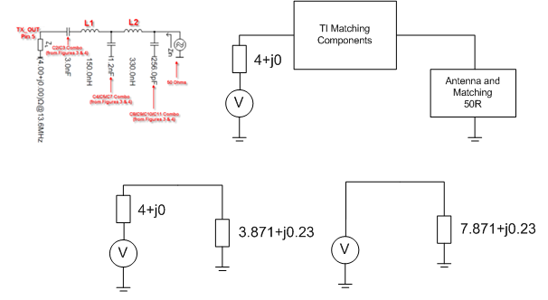
According to the datasheet the absolute maximum Vin pin current is 150mA and typically each supply is derived from Vin. Vin in our application is 5V and we connect VDDRF to VDDPA to provide the antenna supply (as per application examples).

Further down in the datasheet it says the maximum PA output current is 150mA. But there is also mention of 200mW output power capability (assumed into 50R which would be  63mA RMS).

Our antenna coil is a different geometry to the TRF7970A development board but the same inductance and therefore we have the same matching components.

When we simulated the TRF7970A circuit we noticed that the output current from the chip is technically much higher than it is capable of producing (422mA peak).

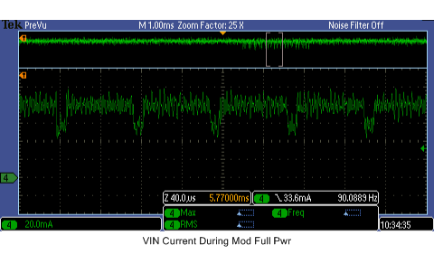
I have measured the output current on the TRF7970A EVM and found that it is 220mA peak (157mA true-RMS from oscilloscope):

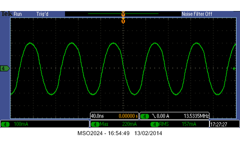
Our circuit (with the same components) shows the same result.

I would like to know if the TRF7970A internally limits the output current to a safe level or if the circuit is operating out of its limits and likely to damage the IC over time.

The theoretical current in the simulation seems to hint that it should be much higher, hence the thought that the chip is limiting the driver current.

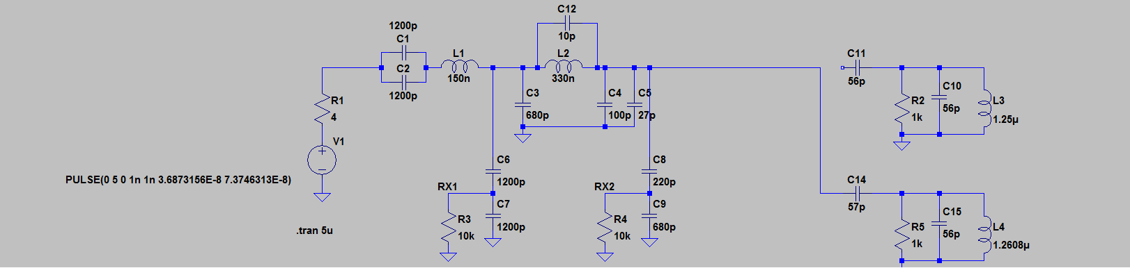
Current above is in R1 (from driver) and 427mA peak.

  • To add to the above, using the EVM the current from the driver pin is 212mA peak (156mA true RMS) with full power setting, 164mA peak (121mA true RMS) with half power setting.

    Is the EVM exceeding the output drive limit of the chip?

  • Sorry to bump up this post but we are under pressure to finalize the design and I am concerned the driver may be overloaded.

    Should I submit this for direct support from TI?

  • Mark,


    I have worked with this part on a shipping product.  I could offer some quick advice and maybe that will suffice.  Otherwise, I could analyze your questions in more detail if needed.

    It looks like you are using LTSpice to analyze your circuit.  One quick comment on your simulation is you assumed all ideal components which is not a good assumption.  Caps have parasitic ESR and ESL although the ESL is not an issue at 13.56 MHz.  Inductors have Q factors (real part) and winding cap.

    I don't have your simulation schematic visible but are you using the same Rx/Tx match TI used?  Also, how different is your "antenna" (actually inductor) to what TI used?

    Have you used any test equipment besides a scope to look at the Tx output?

    Regards,

    Eric Hooker

    RF Consultant

    http://www.linkedin.com/in/erichookerrfconsultant

  • More questions: How did you measure the 212 mA peak driver current at 13.56 MHz?

    Also, have you put a thermal camera on the RFIC?  If so, what is the operating temperature when operating?

    Have you temp tested the RFIC and measured driver current?

    Eric

  • Hi Eric,

    Thank you for your replies. I appreciate the additional parasitics in the real-life circuit that are not present in the simulation. The circuit in the simulation is as per TIs reference schematic and I doubt if parasitics were taken into account during the design of that circuit as it would depend on the end user's physical implementation and component choice.

    In fact they show the derivation of their 4 to 50R matching network assuming ideal components and no parasitics.

    The current was measured using a TCP0030A 120MHz bandwidth current probe with an oscilloscope. I measured more or less the same current on the EVM as our product (they use the same matching circuit and planar coil inductance).

    I haven't temperature tested the IC as I usually like to confirm if I am overrating the recommended design parameters rather than see how hot it is getting on the bench. For example even if the IC is at a low/'safe' temperature I would prefer confirmation from TI that it is ok to pull more current from their output than the datasheet recommends. I am wary of designing off-datasheet!

    The simulation was used in an attempt to back up the theory that the antenna driver would potentially be trying to drive more current than is available at the driver output.

    Interestingly the voltage for the power amplifier is measured at 4V. The datasheet says that the automatic voltage scaling is of the range 4.3 to 5V. I am wondering if the IC tries to compensate for the high output current by scaling down its regulator suppling the power amplifier.

    TI only provide an example for a circuit using 4 to 50R. We are also interested in why a circuit of such small geometry compared to wavelength is concerned with impedance matching for maximum power transfer. For HF we would have thought a series resonant circuit for the antenna drive would be sufficient as per LF reader design techniques.

    I was hoping one of the TI RFID moderators familiar with this device would have measured the output current on their designs to see if they too are potentially overloading the output of the IC. The datasheet just has a statement that the maximum driver current is 150mA.

    Mark

  • Further to the above.

    The TRF7970A datasheet shows how the 4R output driver is converted to look like 50R looking back towards the driver. The antenna is matched to 50R so it looks like 50R looking toward the antenna.

    From a driver current point of view, if you take the antenna as a 50R load at 13.56MHz and work back the impedance that the driver sees looking out from its TX pin you end up with an impedance of 7.871+j0.23 (may have slight rounding errors due to my hand calculations!).

    In the above the 3.871+j0.23 is the impedance seen by the driver including the antenna.

    At 4V drive (the voltage at the driver vreg) you would expect to see around 510mA peak delivered to this load impedance. Hence the output driver of the IC is effectively overloaded.

    I have simulated the full matching circuit (as in my original post) using the true 50R matched antenna and a 4V source and I see 523mA peak from the source supply which ties in with the above derivation.

    So I still need to understand if this suggested circuit is actually overloading the output of the IC as it appears to be internally current limiting in the real circuit.

    The absolute maximum current on the Vin pin is listed as 150mA. The antenna drive is derived from Vddrf connected to Vdda, all derived from Vin.

    The datasheet says 'the maximum output current capability for 5V operation is 150mA'. I am not sure whether to take this as: it will self limit, or I need to design a circuit which doesn't overload the output.

    Mark

  • Mark,

    I think but I'm not 100% sure that the TRF7970A was designed outside the US.  It could be that the TI app engineers here in the US are looking for answers for you but don't have them yet.

    1. Have you measured the Vin input dc current and found that it exceeds the 150 mA abs max?  If not, please measure it and tell us what it is.

    2. What's weird is the abs max input current and the max input current in table 3.4 are both 150 mA.  I have found other issues with the TRF7970A data sheet like this.

    3. What does the TX_OUT voltage waveform look like?  It should be a square wave.  Also, what does the TX_OUT voltage waveform look like when you set the TRF7970A  to half power?  Post scope waveforms.

    4. Have you measured AC current of the driver when the antenna and it's match were replaced with a 50 ohm load?

    Regards,

    Eric Hooker

    RF/Microwave Consultant

    http://www.linkedin.com/in/erichookerrfconsultant


  • Mark,

    I forgot to comment on two other points you made:

    "Interestingly the voltage for the power amplifier is measured at 4V. The datasheet says that the automatic voltage scaling is of the range 4.3 to 5V. I am wondering if the IC tries to compensate for the high output current by scaling down its regulator suppling the power amplifier."  Yes, I think you are probably correct.  This technique is sometimes used for RF power amps. 

    "TI only provide an example for a circuit using 4 to 50R. We are also interested in why a circuit of such small geometry compared to wavelength is concerned with impedance matching for maximum power transfer. For HF we would have thought a series resonant circuit for the antenna drive would be sufficient as per LF reader design techniques." Four ohms to 50 ohms is quite the impedance transformation.  I believe TI used that network so it would not be very sensitive to component tolerances.  Also, notice it is a LP structure and provides harmonic suppression.  I don't know for sure if that's required by the FCC at these low power levels but it may be.  Also, European countries are usually more strict.

    Regards,

    Eric Hooker

    RF/Microwave Consultant

    http://www.linkedin.com/in/erichookerrfconsultant


  • Hi Eric,

    Thanks again for the response - I was hoping TI would have pitched in by now but I guess they may be checking out my observations! I will check some of the above when I am back in the office tomorrow.

    The voltage waveform on the output of the IC has the basic form of a square wave switching between 0 and 4V but has overshoot/undershoot and ringing on each edge - possibly because it directly drives into the coupling capacitance.

    There are loads of issues with the TRF7970A datasheet, you will find a lot posted in these forums. I would have thought it would be an evolution of the TRF7960 series and all the issues ironed-out!

    The TRF7970A (and its predecessors) bear a strong resemblance to the EM Micro EM4094 IC - in fact they have a dual RX structure along with the same matching network. I wouldn't be suprised if they aquired one of the EM engineers! Certainly some of the reasons given for the dual RX structure do not make any sense, but that is a different topic for discussion!

    The EM4094 can be used in a simplified mode with one of the RX pins connected to ground with a decoupling cap and a simple series resonant circuit with single capacitive divider to the main RX pin. It is a good idea to include a LP filter after the output to reduce harmonics and help in the EMC lab!

    Their IC interestingly includes 'antenna short circuit protection' but with little detail. If my theory is correct and the TRF7970A is a clone the I guess it may have some internal current limiting too.

    To be honest I am comfortable with the waveforms and IC operation. I am just concerned that the theoretical matching network they have provided would actually overload the output. Unless I am missing something, the simple transformation of the multiple impedances to a single impedance on the output of the IC is sufficient to prove that point.

  • Hello again Mark,

    I assume you are in the UK or somewhere else in Europe?  I'm just curious.

    Yes, I know about the data sheet issues.  Recall I worked with this actual part just as you are.  I have to say that I never measured the Vin dc current or the driver output current though.  I was actually more concerned with receive mode operation.  You will see a post I left  concerning Rx if interested.

    In my view, if you don't exceed Vin max = 6Vdc -- you keep it at 5Vdc +/- regulator tolerance and you don't exceed the maximum Vin current of 150 mA-dc, then you are okay.  I don't see any spec on driver AC current in the data sheet.  The condition of the dc current spec was Vin = 5V and "operating free air temperature" (-40 C to +110C).  That's why I still suggest you evalaute your circuit over temperature.

    You could always email TI directly about this. 

    Regards,

    Eric

  • Hello Mark & Ray,

    The thermal camera suggestion was only meant to be a troubleshooting tool.  I agree 100% that engineering designs must adhere to all data sheet min and max specifications. 

    Ray, your SPICE schematic is difficult for me to view.  When I zoom in the text is not very clear.  In any event. this thread is concerned with the Tx driver.  Do you have issues with Rx mode operation?  It looks like you are plotting RX voltages... 

    Regards,

    Eric

  • Hi Ray and Eric,

    I am in the UK so a bit delayed with my replies. I am also currently set up to test other aspects of the design but I have measured some of the points you request above.

    Interestingly today I noticed TI have removed the TRF7970A datasheet from the product page! I wonder why and what changes are coming.....

    Ray - I drafted an email to send to you some weeks ago after reading your findings on the dual RX structure after reading your previous posts on the subject. It is an interesting concept that tag presence detection can be used by monitoring each channel RSSI but I do not believe this is the reason for two inputs. I didn't send in the end.

    Some of TIs explanations do not really cover the 'dual RX architecture to eliminate read holes' statement in the datasheet. I have seen many different explanations from TI on this subject. The most plausible seemed to be the one that a previous IC used to need you to set up a delay for sampling the received data to compensate for the phase shift between the TX clock source and received data. By having two inputs you have two signals out of phase so if one doesn't appear to read with your particular system the other probably will.

    Interestingly both TI and EM sometimes say the dual RX is to allow 'phase modulation' to be detected, not that any tags use this. In fact both manufacturers also call the bit that determines which input to use 'PM' for 'Phase Modulation'! I wonder if anyone really knows why there are two inputs!!

    Anyway, back on the main thread subject of the output drive. The Vin pin current is within spec - the trace below shows repeated reads with a small pause between each, around 80mA.

    The antenna pin current and drive waveform are shown below. Note the drive voltage at the pin is attenuated. It seems you can't accurately model the output as a voltage source with 4R load as it seems to have a more complex limiting structure. The current is 212mA max and 150mA RMS. The voltage waveform details can be found in the cursor box top right.

    I also measured the current waveform at the point of the 50R match to the coil:

    I will measure the current in the coil too. I can't really give you voltage measurements as the probe capacitance would distort the figures.

    PS I used a thermal imaging camera in a previous job for fault finding but unfortunately our test equipment budgets do not stretch that far at my current employer!

    Hopefully TI reply soon with some information. It will be interesting to see why the datasheet has been taken off the website.

    Mark

  • Mark,

    If you are set for full Tx power then 80 mA dc current is too low.  Were you set to half power? The data sheet spec for half power Tx is 78 mA maximum -- close to your measurement.  Full power Tx supply current should be 130 mA typ, 150 mA max.

    BTW, since currents and voltages change as impedances change, I wonder if that was the reason for your driver output concerns?  (Since driver current at 4 ohms will be higher than current into 50 ohms.)

    The data sheet is on the web now -- it's dated 19-Feb and at rev I.  I didn't look it over to see what was changed.

    Eric

  • Eric,

    I drafted a full reply but just as I went to post the E2E forums went into maintenance mode!

    The datasheet link is dated 19th Feb but if you click on the link it still brings up the previous rev datasheet (H, Dec 2013). I have reported this to TI.

    The chip is set to full power mode although I haven't yet repeated measurements set to half power. I am happy with the functionality of the chip and understand the various modes / circuit design.

    My main concern here is with the loading at the output of the IC and I am hoping at some point TI will confirm my theory above. Ray has simulated the circuit too and sees the same high theoretical current. I think from this we can conclude that the output driver is not just a source with a 4R resistor as modelled and actually performs some dynamic scaling of the output drive level.

    I am hoping someone else looks at the network applied to the output of the IC and also confirms my calculations and simulations that show that this looks like around 3.87+j0.23 load. I guess only TI will know if this has any effect on the driver.

    My guess is that as their are probably many designs out there based on their driver circuit no one has noticed this and everything runs fine. However, we are about to launch a volume product based on this so I need re-assurance when something appears out of the datasheet that it is safe to proceed.

    I am surprised I haven't had a response from either of the TI RFID forum moderators - I see they have been replying to other posts. I guess I may need to go direct for support rather than use forums.

    Thanks, Mark

  • I don't understand why the 5V dc current is so low if you're at full power.  Have you ever connected the 50 ohm output into a spectrum analyzer of a RF power meter?  I did when I worked on it and the power was as expected.  Maybe you are not putting out the power you think you are.

    I've looked at the match on a RF simulator.  I can post the results later.

    Eric

  • Meant to write: spectrum analyzer or a RF power meter.

  • Ray,

    Yes, I have already analyzed this circuit on a RF linear simulator.  I will post results in about 4 or 5 hours.  I have plans for the evening here in the US.  ;)


    BTW, have you measured the Tx output power using a spectrum analyzer and/or RF power meter?  (At the 50 ohm point of course.)

    Regards,

    Eric

  • All,

    The Tx match was simulated with a s-parameter simulator and then plotted with Sonnet.  The caps were modeled as series RLC.  The 1008CS inductors used measured Coilcraft s-parameter files.  Below is looking into the 50 ohm point towards the Tx output.  If Tx output return loss could be measured, it would look like this.


  • I tried to post a reply but got a response that posts to this forum must be approved by a moderator first.  What I tried to post was a s-parameter plot showing the match from 4 ohms to 50 ohms looking into the 50 ohm port.  The simulation predicted a 19.4 dB return loss which is pretty good.  Let's see if this post appears or not.


    Eric Hooker

    RF Consultant

  • Okay, that last post appeared.  Here's the plot

  • I can't seem to paste plots from Sonnet so attached is a Word file with the predicted match into 50 ohms.  As I wrote above, it looks pretty good -- about 19 dB return loss.  Let's see if the Word file is accepted.


    Regards,

    Eric Hooker

    8322.TRF7970A Tx match into 50 ohms.doc

  • Attached is another Word file showing the simulated impedance at the TX_OUT pin.  The simulated impedance at 13.6 MHz is 4.95 + j0.69 ohms which is off a bit from the desired 4 + j0 ohms.  But, I don't believe this should be much of a concern.  It could be improved by cap tuning if desired.

    Again, the 0603 cap models were series RLC and the Coilcraft 1008CS inductors were modeled with measured s-parameters.

    Eric

    5270.TRF7970A impedance at TX_OUT pin.doc

  • Ray,

    Yes, I thought Mark must have been set to TX low power based on his Vin dc current measurement.

    I have also simulated the TX_OUT match with SPICE and viewed the voltage and current waveforms.  The problem is we don't have a good model for the TX driver -- it doesn't behave as a simple square wave generator with a 4 ohm output impedance as Mark showed with his lab plots.  So, SPICE can't predict the waveforms if the driver model isn't correct.  I'm still interested in the Vin dc current when the TX is set to full power.


    Regards,

    Eric

  • Hi Guys,

    Sorry for the timezone delay! I can see my original post has brought up a lot of topic for discussion.

    Following basic circuit theory and looking at the true measurements I think we can conclude that the output of the TRF7970A is limiting the load current. It has to be because:

    1. The theoretical load applied analysing the output circuit should be drawing more current
    2. The VDDRF regulator can supposedly supply 150mA to the PA according to the datasheet (smoothed by decoupling to some extent from a higher peak value)
    3. 150mA is less than the theoretical current assuming a 4R source to our matching components/antenna

    So for one I need to know that the above is ok.

    We also cannot accurately model the behaviour in spice because of this. For example it appears the VDDRF regulator is scaled down to 4V feeding the PA. We do not know if TI add series impedance or control the turn-on of the mosfet to limit the current.

    We do know that they can provide different modulation depths to the transmitted signal so they must be able to dynamically control the drive strength on the output pin to a higher level.

    I have read that the TRF796x range turn on their output during the start-up sequence to automatically adjust their internal regulators. Presumably this is done for 'max power output' setting. If I measure VDDRF output voltage it is 4V so clearly the IC has scaled its output drive down because of the load on the output. Interestingly this is below the minimum setting of 4.3V.

    I can confirm that the chip is in fact at full power for all of the measurements to date. If I switch to 'half power' mode then the input current drops a bit:

    (white is Vin pin current full power, green is half power)

    I don't think you can use the expected currents in the datasheet unless you really know for sure how they are measured. I am trying to make the point that the theoretical load is greater than expected which could completely distort measurements by distorting the output driver and the resulting input currents.

    FYI, note in the above the change in green trace current just after centre. These dips in current are due to the output modulation talking to the tag as the IC increases the output driver impedance to reduce its amplitude. There is approx 5ms delay before this which was a coding error and been reduced to 500us now.

    You can see below the Vin pin current when the output modulates data to the tag dipping with the modulation.

    Interestingly we have the TRF7970A set to OOK but it appears to be amplitude modulating its output (looking directly at the tx pin) with around 50% modulation depth. This is another issue to look at - I would expect the output to be gated on/off for OOK.

    In response to the requests for more measurements for now I am still waiting for TI to provide information on the output structure and what it is doing with the load implied by the matching network. You can see the same measurements on the EVM so they should be easy to reproduce.

    I could replace the coil for 50R resistor but I do not see the point as I have checked my coil matching looks like 50R with a VNA.

    I cannot replace the output structure with 50R because it is not, certainly not from the TRF7970A's viewpoint.

    It is difficult to know how to proceed without TI getting involved to explain more about the output structure. We know if is not 4R and must be current limiting. Another test could possibly be to supply VDDPA from a higher current external source and not the VDDRF regulator but I am not sure about doing this. The output is either being restricted by the output driver or the regulator supplying the output driver.

    Mark

  • Mark,

    Plenty of useful information was posted here.  I'm moving on to other topics now.  Best of luck with your NFC designs.

    Regards,

    Eric Hooker

    RF Consultant

    http://www.linkedin.com/in/erichookerrfconsultant

  • I am reposting following a request to the Direct TI Support who said that if I bump up this thread one of the TI RFID Experts would read it and answer my request.

    As stated at many points in this post I am trying to find out if the TI output is being overloaded by the matching network suggested by TI and if it is in current limit.

    This thread has become a bit clouded with other responses but the whole point of it was to get agreement that the output matching network provides a load at 13.56MHz that would pull more current from the TRF7970A than recommended and that the output must be current limiting for this to occur.

    Please could someone from TI respond with some input to this? 37 posts and 661 views to date and I cannot attract an answer from TI where other posts are getting rapid responses.

    Regards, Mark

  • Hi. I have not yet had a response from ti technical support or via the forums on my enquiry. I am not sure where to go next to get an answer?!

    please could someone from TI offer advice or at least some comment on my findings in this thread?

  • Mark,

    Have you tried calling and/or emailing TI directly about this?  If not, one great resource at TI is Josh Wyatt.  His email is Josh.Wyatt@ti.com


    Regards,

    Eric Hooker

  • I sent an email directly to Josh on 17th Feb, no response as of yet.

    I registered this with TI direct support a couple of weeks ago and the response was to bump up the thread and someone from TI would reply - I have done this twice now and still no response.

    I may create a clean thread as my message is a bit lost in all of the replies. The main point being the load applied by the matching circuit to the IC (regardless of measurements on live board, using circuit theory is enough to understand my point).

  • They probably don't have the answer then or are still waiting for it.  You may have to talk to the IC designer if possible.

    Another idea is to characterize the TX driver yourself.  Connect various loads to it and measure the response.  You may get a better understanding of the driver this way.

  • I got a phone call from TI tech support. The excitement was short lived when the guy suggested that I now contact a local distributor for their FAE support.

    I explained that my question is really aimed at someone with knowledge of the silicon so I was hoping for a TI internal response.

    He then mentioned that the forums are a good place to go for support.....

    I am not characterising the driver myself because my question is if the output of the IC is being overloaded past its design margin. I can't possibly say if I am exceeding the silicon design limitations because I do not know what these are. I also do not know what aspect of the design is acting as the limiter - internal LDO, output driver?

    I do not want to guess. All I am interested in is a response to explain whether there is a problem.

  • mark - 

    what is your contact info? i cannot find an email from you in my inbox or archive (and i don't delete emails)

  • Hi Josh,

    I have resent the email to your public TI email address on your forum profile (josh.wyatt@ti.com). I hope you are able to help me with this query.

    Thank you.

  • Hi Mark,

    I have read the entire post and I have encountered the same problem as you to get a TX model for LTSPICE. Have you received any news/answer?

    My schematic is similar to yours. The only difference is that I consider 4ohm resistance as part of the source voltage , so that for a voltage V1=5V, the measured voltage with the probe is about 2.5V, due the internal resistance.

    Sorry, if my english is not pretty good.

    Best regard,

    Luciano Martínez Rau
    luciano.mrau@gmail.com
  • Hi Josh,

    I apologize for resurrecting this ancient discussion... and I appreciate that you've posted the LTSpice models that you use, but I am now fully confused.

    The datasheet claims that the TRF7970 should have an output power of 200mW but using the spice models you've posted I see much higher output power (around 600mW).. Could you explain?

    I read through all of the previous posts on this thread contemplating how the drive circuitry actually works to get to 200mW, but it seems that the LTSpice model you shared show that it doesn't? Or maybe I am just confused.

    Thank you,
    Eric Horton
  • into 50Ohm load, we would look at the Vpp and resulting calculated Vrms, then calculate power from there. 

    so on slide 9  of the attached. you will see we measure about 9.6Vpp, which calculates to 3.39Vrms 

    using P = Erms(squared) / 50 = 0.230W or 230mW, or 23.617dBm  - OK?

    0878.TRF79xxA_Test points_05_2013.pdf

  • Okay that makes sense as far as output power from the coil is concerned.

    I am making my own PCB based coil for the TRF7970A and I was trying to determine what kind of current range I should be seeing on TX pin to ensure that I am not damaging the IC.

    Would you just suggest measuring outputs from the evaluation board/LTSpice model and then just comparing to my prototype? Or is there some limit that the TX pin should not be driven past (couldn't find on datasheet)?

    In other words: Does the TX pin have some maximum output current that it regulates itself too, or could a mismatched antenna damage the IC.

    Thanks,
    Eric
  • a mismatched antenna would possibly damage the part over a long period of time, but you would catch it well before that because the main symptom that would manifest would look like firmware problem - i.e. you would have poor performance that may look like the interrupt handler is broken, etc.
  • Hello Mark

    All that you saidn is interesting for me. and I would like to raise some small question about how you measure these values? I mean which pin do you use ? which load impedance do you consider ? and how to switch TI in half power mode?

    Thanks
    Mossaab