This thread has been locked.

If you have a related question, please click the "Ask a related question" button in the top right corner. The newly created question will be automatically linked to this question.

CC2540 PCB revision

Hello!

We are making pcb for BT4 RGB led driver. We already made our first prototype, but BT was not functioning, probably because PCB was only 2 layer 1.6 m thick, so there was no way to provide 50 ohm caracteristic impedance for RF tracks.

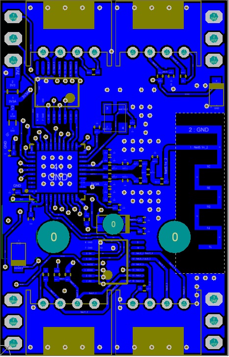
I'm posting image of second revision, which has 4 PCB layers. I would like to hear your comments and if I should correct pcb routing.

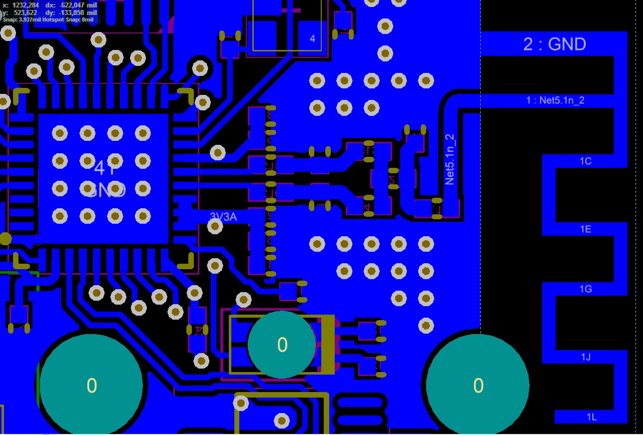
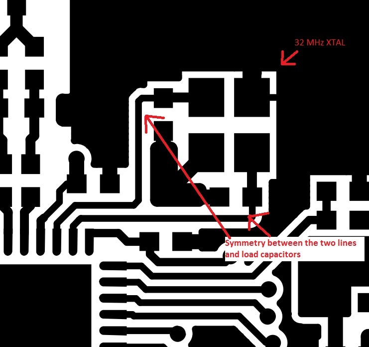
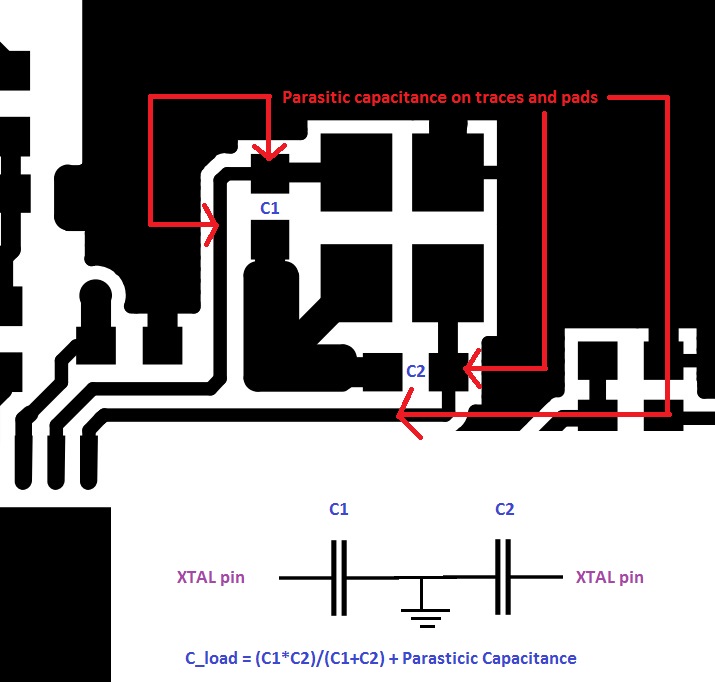
This is top layer, of RF portion of circuit. Underneath ths layer is solid copper pour. Components that form a balun are placed exactly as in reference design (http://processors.wiki.ti.com/index.php/SAT_-_Gas_Sensor_Platform_with_Bluetooth_Low_Energy).

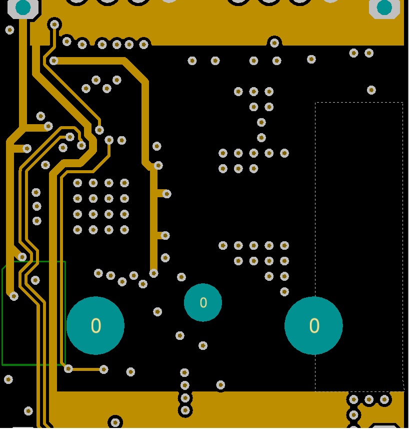
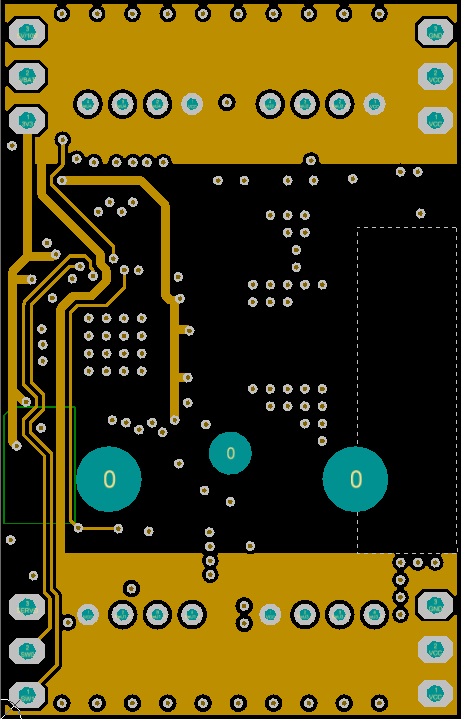
This is layer that has power suply lines. On this image it can be seen, that no track runs under RF section.

  • Hello Matjaz,

    If i see correctly you do not have any proper ground plane under neath the chip or RF lines. I see all the vias under the chip, but they don't seem to be connected to ground. If this is the case you have no chance of making it work properly. 

    Does the 32 MHz crystal oscillator start up?

    You can test this by checking registers or outputting the clock on GPIO pins and measure it with an oscilloscope or logic analyzer.

  • Hi Eirik,

    Probably I wasn't clear in the first post, but PCB will have 4 layers, I just didn't post the image of ground plane an bottom layer. So to remove any comfusion, here are the images of all 4 layers as they will be in layer stackup:

    PCB will be made out of single core (thicknes 29.9mil), and prepreg thicknes will be 13.7 mil, which should give about 50 ohm caracteristic impedance of track that is 20 mil wide.

    I do belive that oscillator starts up, because we were able to connect the board to the CC DEBUGER and comunicate with it.

  • Hello Matjaz,

    At a first glance i think the layout looks quite good. The ground planes look good. When you have such short RF lines between the balun and the antenna (less than 10% of the RF wavelength) there is a rule of thumb that characteristic impedance is close to negligible. Characteristic impedance (or distributed theory) is based on the notion of having a phase shift along the line which can cause issues when you have reflections propagating through it , but in this case there is almost nor phase delay.

    The debug interface is not dependent upon the 32 MHz clock. The chip will start the internal 16 MHz RCOSC as system clock at start-up (This cannot be used for RF operations). You should start by checking this. This can easily be done by using some of our available source code and looking in to the "clock set" functions. After you set the clock you can check the CLKCONSTA register to verify of the clock source has successfully changed to 32 MHz. Also look at the picture below to see our crystal layout recommendation. You want the two lines to have relatively equal length. 

    If the 32 Clock source works well i would investigate the BalUn, what kind have you used? Is it properly connected/mounted?

  • Thank you for your answers Eirik!

    On first revision of pcb we meant to use Murata’s LFB182G45BG2D280,but it was out of stock on Mouser  and other electronic sulyes dealers so we went with DEA202450BT-7210A1 from TDK.

    On this revision we will be making  balun from discret components (inductors and capacitors) as described in this AppNote:  http://www.ti.com/lit/ug/snoa922/snoa922.pdf

  • Ok, sounds good :).

    Also remember to check the load capacitance on the 32 MHz Crystal. If you have used another than in our reference design you might need to change the value of the load capacitors.

  • Indeed we are using difrent crystal, CX3225GB32000P0HPQZ1 from AVX. In this datasheet: http://global.kyocera.com/prdct/electro/pdf/xtal/cx3225gb_cs_e.pdf it says Load capacitance: 8pf. This is the value of capaicotrs we should use on our board right?

  • Hello Matjaz,

    Yes, that will be close.

    The total load capacitance is calculated from the PCB board parasitic (capacitance) and the two capacitors which is seen as two in series from one of the pins through ground then through the other capacitors connected through the other pin. It is difficult to measure the specific parasitic capacitance on the board, but an estimated guess for designs similar to our ref designs may be 2-4 pF ( might deviate from this on different designs). 

    For your case your two 8pF caps will end up as a total of 4 pF (two caps of equal size in series will effectively be half the value  when combined, just think of the equation for parallel plates capacitors and double the distance (linear dependency) you will end up at half the value. Then if you have around 3-4 pF in parasitics, you will end up around the desired 8pF. I tried to draw a simplified explanation below: