This thread has been locked.

If you have a related question, please click the "Ask a related question" button in the top right corner. The newly created question will be automatically linked to this question.

CC1101 + CC1190 EVAL BOARD: POWER AND BANDWIDTH

Other Parts Discussed in Thread: CC1101, CC1190, TEST2

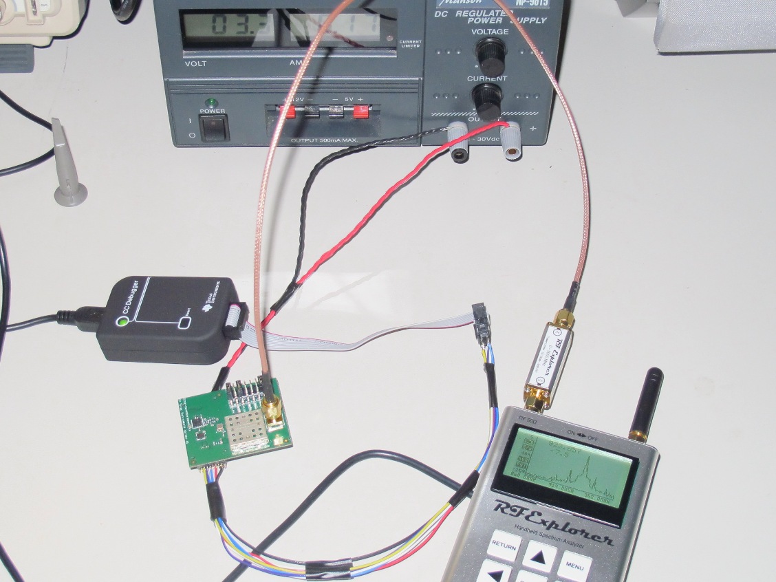
I have recently purchased CC1101CC1190EMK915 evaluation board for CC1101 and CC1190 at 915MHz band.

I am using an XMEGA-A3BU Xplained demo board to talk to the RF board for evaluation purposes (should not impact these observations).

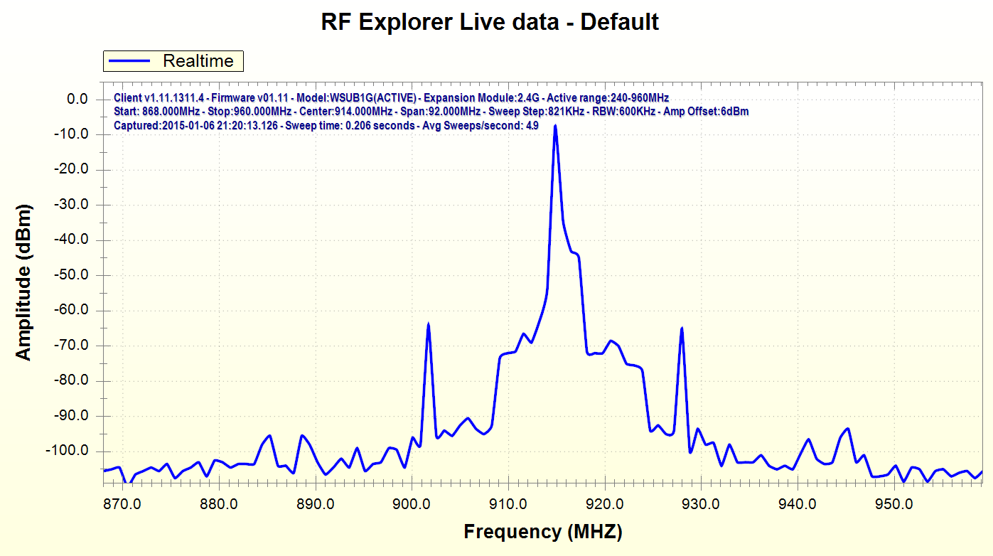
During initial testing, I was only able to achieve 300m max range from the units using simple low bit-rate data transmission (using values from smartRF studio). This seemed curious since these units should be able to provide km's of range (so I hear). To investigate further, I connected the RF output of the eval board to my RF Explorer and set the CC1101 to transmit a continuous wave (OOK with both on and off set to same power level - as per smartRF studio).

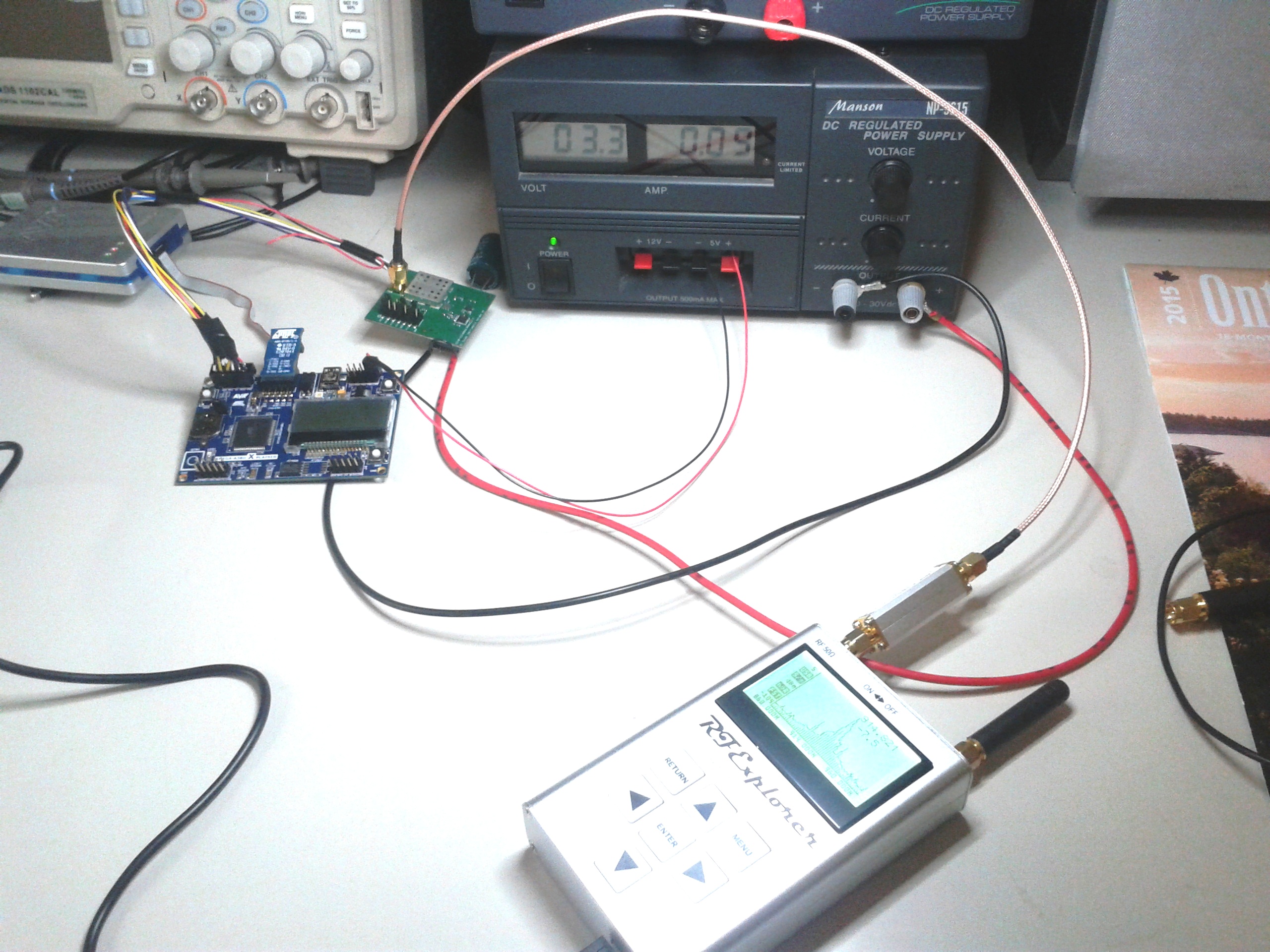
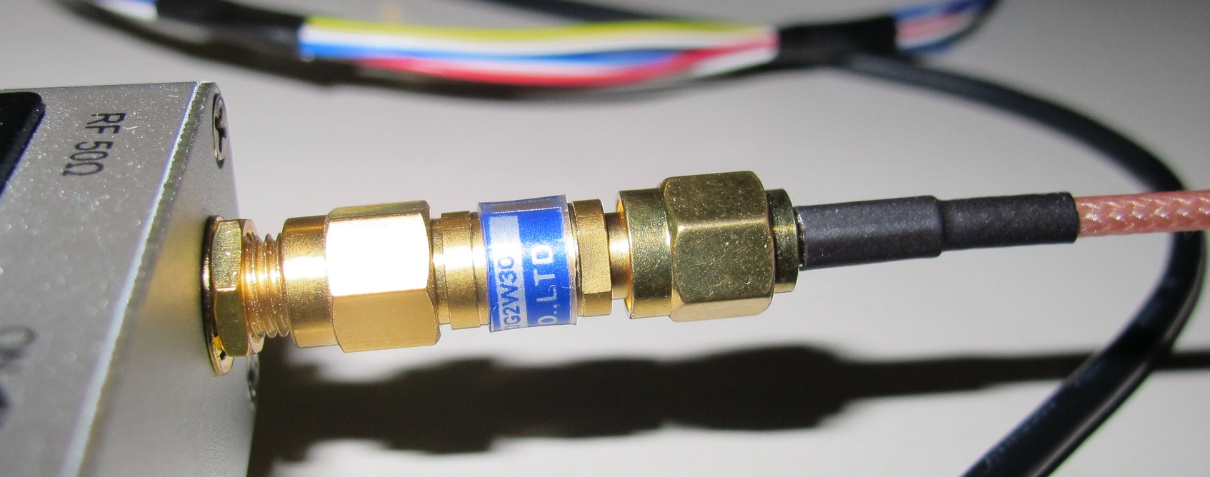
The CC1101-CC1190 eval board is connected to it's own power supply capable of supplying 5A with thick (2mm^2) wires. Both positive and all three ground terminals are connected from connectors P1 & P2. Connection to XMEGA via SPI port and two independent GPIO's for PA/LNA control. I have verified the SPI communication and ability to set registers in the CC1101. Operation of PA and LNA have also been confirmed. The rectangular box on top of the RFexplorer provides 6dB of attenuation which is accounted for with internal settings.

I then took peak readings for a range of RF output powers (set in PATABLE registers), however I was not able to produce any more than approx -8dBm. Adjusting the PATABLE settings from -20dB to +5dB (output of CC1101 - input to CC1190) only varied this maximum power by about 2-3dBm??? Therefore I can see that the full power is not being delivered properly. Interestingly, the power consumption of the device actually matched closely to the datasheet during these tests (90mA - 260mA) with higher power settings drawing higher currents. So where is this power going?

When we look at these plots, it can be seen that the peak amplitude varies very little, but the bandwidth (frequency spread of the transmitted signal) increases with higher powers. So it looks like the energy is not being "focused" into the centre frequency, but rather just spreading out sideways.
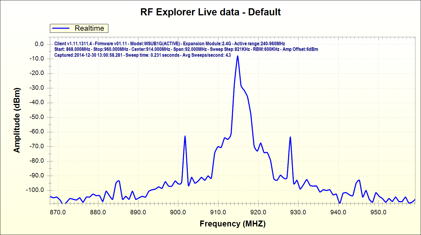
PATABLE 0x0E -20dBm

PATABLE 0x8E 0dBm

To be honest, both of the above plots seem to consume too much bandwidth.

Can anyone suggest why this may be occurring and how to resolve it to produce higher output power and range?

  • SETTINGS FOR CONTINUOUS WAVE:
    halRfWriteReg(FIFOTHR,0xC7); //RX FIFO and TX FIFO Thresholds
    halRfWriteReg(PKTCTRL0,0x12);//Packet Automation Control
    halRfWriteReg(FSCTRL1,0x06); //Frequency Synthesizer Control
    halRfWriteReg(FREQ2,0x23); //Frequency Control Word, High Byte
    halRfWriteReg(FREQ1,0x31); //Frequency Control Word, Middle Byte
    halRfWriteReg(FREQ0,0x3B); //Frequency Control Word, Low Byte
    halRfWriteReg(MDMCFG4,0xF5); //Modem Configuration
    halRfWriteReg(MDMCFG3,0x83); //Modem Configuration
    halRfWriteReg(MDMCFG2,0x30); //Modem Configuration
    halRfWriteReg(MDMCFG0,0xF7); //Modem Configuration
    halRfWriteReg(DEVIATN,0x31); //Modem Deviation Setting
    halRfWriteReg(MCSM0,0x18); //Main Radio Control State Machine Configuration
    halRfWriteReg(FOCCFG,0x16); //Frequency Offset Compensation Configuration
    halRfWriteReg(WORCTRL,0xFB); //Wake On Radio Control
    halRfWriteReg(FREND0,0x11); //Front End TX Configuration
    halRfWriteReg(FSCAL3,0xE9); //Frequency Synthesizer Calibration
    halRfWriteReg(FSCAL2,0x2A); //Frequency Synthesizer Calibration
    halRfWriteReg(FSCAL1,0x00); //Frequency Synthesizer Calibration
    halRfWriteReg(FSCAL0,0x1F); //Frequency Synthesizer Calibration
    halRfWriteReg(TEST2,0x81); //Various Test Settings
    halRfWriteReg(TEST1,0x2D); //Various Test Settings
    halRfWriteReg(TEST0,0x09); //Various Test Settings


    SETTINGS FOR RANGE TESTING:
    halRfWriteReg(FIFOTHR,0xC7); //RX FIFO and TX FIFO Thresholds
    halRfWriteReg(PKTCTRL0,0x05);//Packet Automation Control - Variable packet length and CRC enabled
    halRfWriteReg(FSCTRL1,0x06); //Frequency Synthesizer Control
    halRfWriteReg(FREQ2,0x23); //Frequency Control Word, High Byte
    halRfWriteReg(FREQ1,0x31); //Frequency Control Word, Middle Byte
    halRfWriteReg(FREQ0,0x3B); //Frequency Control Word, Low Byte
    halRfWriteReg(MDMCFG4,0xF5); //Modem Configuration
    halRfWriteReg(MDMCFG3,0x83); //Modem Configuration
    halRfWriteReg(MDMCFG2,0x13); //Modem Configuration
    halRfWriteReg(MDMCFG0,0xF7); //Modem Configuration
    halRfWriteReg(DEVIATN,0x31); //Modem Deviation Setting
    halRfWriteReg(MCSM0,0x18); //Main Radio Control State Machine Configuration
    halRfWriteReg(FOCCFG,0x16); //Frequency Offset Compensation Configuration
    halRfWriteReg(WORCTRL,0xFB); //Wake On Radio Control
    halRfWriteReg(FSCAL3,0xE9); //Frequency Synthesizer Calibration
    halRfWriteReg(FSCAL2,0x2A); //Frequency Synthesizer Calibration
    halRfWriteReg(FSCAL1,0x00); //Frequency Synthesizer Calibration
    halRfWriteReg(FSCAL0,0x1F); //Frequency Synthesizer Calibration
    halRfWriteReg(TEST2,0x81); //Various Test Settings
    halRfWriteReg(TEST1,0x2D); //Various Test Settings
    halRfWriteReg(TEST0,0x09); //Various Test Settings
  • Your settings look ok, but from the picture, it seems that your jumper settings for the control of the CC1190 are not correct if you want to use the GPIO pins to control the LNA and PA enable. However, I can not see where you connect your wires, but can you please confirm that you have checked the jumpers with respect to where you connect the wires?
  • Here is a close up of the jumper settings:

    Here is also an image of the PCB connections where the PA and LNA are connected (white and purple wires on very right)

  • That looks ok, since your not using the GPIOs on the CC1101 to control CC1190. Do you have a TRXEB or similar that you can try to control the EM using SmartRF studio, just to control that the HW is ok?
  • No I don't, but I have tried with both boards from eval kit and have the same results. I also have two Xmega boards and they both show the same results.

    If the units are pulling the higher current (say 250mA) it seems that the unit is "trying" to transmit right? So why wouldn't the centre frequency amplitude increase?
  • It all sounds strange and I am not able to reproduce your observations in the lab using SmartRF studio. Do you have a regular CC1101 EM to test or a CCdebugger so that you can control your EM with SmartRF Studio?
  • I have ordered a CCdebugger as suggested for testing purposes.

    The only issue I observed during development was that I was unable to get the CC1101 to manually reset according to section 19.1.2 of datasheet. I was never able to observe the CC1101 chip pulling the SO line low after the CSn sequence was completed.

    Could this be contributing to the problem? I am still able to write to all the registers, but perhaps some registers contain values which need to be cleared? I would assume that this would be taken care of during each power up?
  • The CC1101 has a automatic POR, but it is very interesting that you do not get the SO line low after the CSn sequence was completed when running a manual reset, the SO line must go low to be sure the chip is ready. Otherwise you can get a undefined behavior. Do you have a plot or similar from a logic analyzer showing the SPI interface when running the manual reset? How do you verify that you can set the registers correct, have you read the registers after setting them?
  • Here is a photo from my oscilloscope. The yellow line is the CSn wire and the blue line is the SO wire.

    You can see that there is more than 40us between the two CSn high-low transitions. CSn has been held high for 5ms preceding the first high-low transition.

    I can confirm that the SO wire is working since I see signals there during SPI communications later in program execution. None the less, my code then issues the SRES command strobe until the chip status byte returns 'idle' and then proceeds.

    The registers are reading back correctly after being set as confirmed using xmega debug.

    I have confirmed the voltage levels on CC1190 control set by GPIO are as follows for continuous TX mode:

    LNA_EN = 0V

    PA_EN = 3.3V

    HGM = 3.3V

    This is very confusing...

  • Here you can see the same CSn and SO wires as the code continues to execute (above image used a breakpoint in debug to stop code execution):

  • Do you have a plot showing the manual reset and also showing the SI line and the SRES command strobe? The low SO signal indicates that the XOSC is ready and stable, so that is ok, but you should get a transision of the SO signal during the SRES  command strobe.

  • CC Debugger arrived today. I have connected the debugger to the device according that suggested in CC debugger datasheet figure 10. After updating the CC debugger firmware to 044 it recognised the CC1101 and the led turned green:

    RF Studio recognised the debugger and I was able to make the following settings:

    The power supply was supplying approx. 150mA during this mode setting. The transmission was visible on my RF Explorer and here is a screen dump:

    Again the output power was only -7.5dBm at its peak (not 20dBm as set in RF studio).

    This is leaving me scratching my head... Any further thoughts?

  • Ok, so I decided to switch out the 6dB RF attenuator for a 30dB attenuator I purchased from Ebay:

    The RF explorer now shows +14dBm signal! The power supply is also now showing approx. 200mA current. Here is a screen shot:

    Looks like the problem was mainly the attenuator. However the reading is still -6dBm from the RF studio settings. Perhaps some signal is being lost in the 30cm cable I am using. I will replace this next to see if this improves the situation.

  • I am surprised you are still getting low output power, if you send from one EM to another with some attenuators in between, how does the RSSI level for the EM in receive look like? Do you have a signal generator or another known transmitter that you can use to check the level of the spectrum analyzer you are using? How does the spectrum look like if you configure it to continuous TX and unmodulated carrier?