This thread has been locked.

If you have a related question, please click the "Ask a related question" button in the top right corner. The newly created question will be automatically linked to this question.

CC1101 datasheet discrepancy

Other Parts Discussed in Thread: CC1101

We are having troubles with the CC1101 and found an apparent discrepancy on the datasheet for this part.

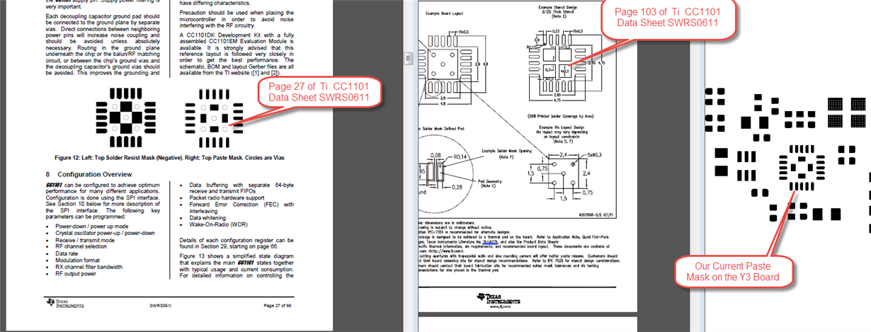
Page 27 of the SWRS0611 seems to indicate a soldermask opening with a square pad located north center, west center, east center, and south center on the center ground slug. This image has no dimensions.

Page 103 of the same datasheet has beautifully dimensioned drawing of the stencil and is a bit vague on the soldermask opening requirements, however given the stencil design, it is possible to imply intended soldermask requirements. It seems that this drawing is more detailed and specific and in accordance with many other device stencil/solder attach designs.

Since we are having production issues with this, we are investigating any area where there is area for concern. Since my first review of this design, I have been concerned with this exposed pad and stencil strategy. 

I have attached an excerpt from your datasheet for reference. I would like to get an explanation of which method is preferred and a rationale for using each type of both are acceptable. It appears that both thermal and RF ground would be better served by the stencil/pad design on Page 103.


Looking forward to a comment from TI.

  • From my understanding this is due to historical reasons but it should have been the same at both places in the datasheet. The drawing on page 27 is what we used in Chipcon and is what we have used on our reference designs. Page 103 is what TI recommends for that type of packet.

    Both patterns will work.

    Note that your assembly house need to dictate the exact size of the solder paste since the amount etc will be dependent on that specific production line. Not enough solderpaste will cause poor grounding, too much and the chip will "wobble" and have connection problems. If you suspect the soldering, take a xray to see how the chip actually is connected.
  • As TER explained, the example on page 27 should be followed.  The diagram on page 103 is a generic drawing, used for hundreds of devices, and for the CC1101, what we have discovered by actual practice, this generic model has to be modified.  The actual solder mask and paste files are in the EM Ref Design ( http://www.ti.com/litv/zip/swrr046a ) .  In the Reference Designs we have placed vias inside the exposed die attached pad (see pg 7 for paste, pg 11 for mask). These vias should be "tented" (covered with solder mask) on the component side. We recommend using dots for the paste layer so that the central pad is not covered 100% with paste.  Coverage should preferably be around 70%, the important thing is to get a good solder bondThe recommended soldering profile for CCxxxx products is according the IPC/JEDEC J-STD-020B or the CECC 00802, Edition 3.